Multilayer ceramic electronic component

a technology of electronic components and ceramics, applied in the direction of fixed capacitor details, stacked capacitors, fixed capacitors, etc., can solve the problems of time and effort required for the development of ceramic materials of high functionality, the capacity of multilayer ceramic capacitors has become larger and larger, and the development of ceramic materials with high functionality requires time and effort. , to achieve the effect of increasing electrical strength, greatly reducing electrical strength, and increasing electrical strength

Active Publication Date: 2012-10-04
MURATA MFG CO LTD
View PDF6 Cites 16 Cited by
  • Summary
  • Abstract
  • Description
  • Claims
  • Application Information

AI Technical Summary

Benefits of technology

[0015]In still another preferred embodiment of the multilayer ceramic electronic component according to the present invention, the plurality of first internal electrodes may be exposed to the third surface, ends thereof adjacent to the fourth surface may not be exposed to the fourth surface, the plurality of second internal electrodes may be exposed to the fourth surface, and ends thereof may not be exposed to the third surface. Each of at least the plurality of first internal electrodes or the plurality of second internal electrodes may include a saddle in an end adjacent to the fourth surface or the third surface, the saddle being thicker than a remaining portion of the internal electrode. Of at least the plurality of saddles in the plurality of first internal electrodes or the plurality of saddles in the plurality of second internal electrodes, at least one saddle of the plurality of saddles may not overlap remaining saddles in the third direction. In this case, in production of a ceramic sintered body, when an unfired ceramic stack is pressed in the direction in which the first and second internal electrodes are stacked and the ceramic layers are closely attached to each other, a difference in level is less likely to occur in the ceramic stack, in comparison with the case in which all saddles overlap each other. Accordingly, delamination is unlikely to occur after firing. Thus, the electrical strength can be increased.
[0016]In another preferred embodiment of the multilayer ceramic electronic component according to the present invention, a ceramic layer disposed between the first and second internal electrodes facing each other may preferably have a thickness within a range of about 0.3 μm to about 2 μm, for example. In this case, because, if a bend having a plurality of inflection points exists, the electrical strength greatly decreases, the present preferred embodiment is especially effective.
[0017]In another preferred embodiment of the multilayer ceramic electronic component according to the present invention, a ceramic layer disposed between the first and second internal electrodes facing each other may preferably have a thickness within a range of about one to about three times a thickness of each of the first and second internal electrodes, for example. In this case, because, if a bend having a plurality of inflection points exists, the electrical strength greatly decreases, the present preferred embodiment is especially effective.
[0018]In various preferred embodiments of the present invention, no bends including a plurality of inflection points exist in ends of each of the first and second internal electrodes adjacent to the fifth and sixth surfaces. Therefore, even when the ceramic layer between the first and second internal electrodes is thin and the number of stacked layers is large, a decrease in electrical strength is minimized or prevented. Accordingly, both miniaturization and high electrical strength is achieved.

Problems solved by technology

In recent years, multilayer ceramic capacitors have become smaller and smaller and their capacities have become larger and larger.
Unfortunately, the development of the ceramic material having high functionality requires time and efforts.
Unfortunately, the multilayer ceramic electronic component in which the ceramic layers are thin, the number of stacked layers is large, and the opposing area of the internal electrodes is large suffers from low electrical strength.

Method used


Image

  • Multilayer ceramic electronic component
  • Multilayer ceramic electronic component
  • Multilayer ceramic electronic component

Examples


first preferred embodiment

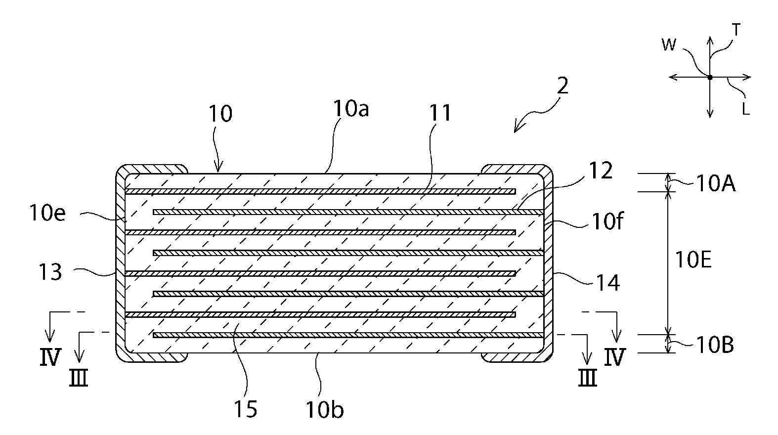
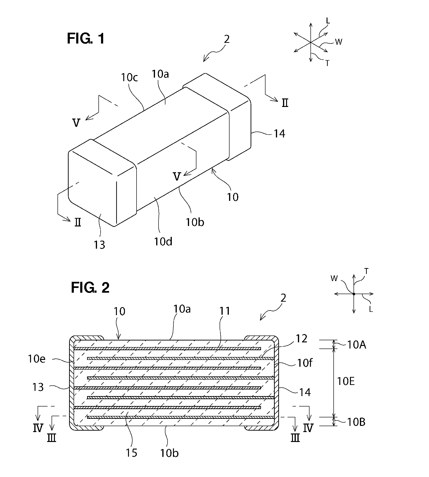
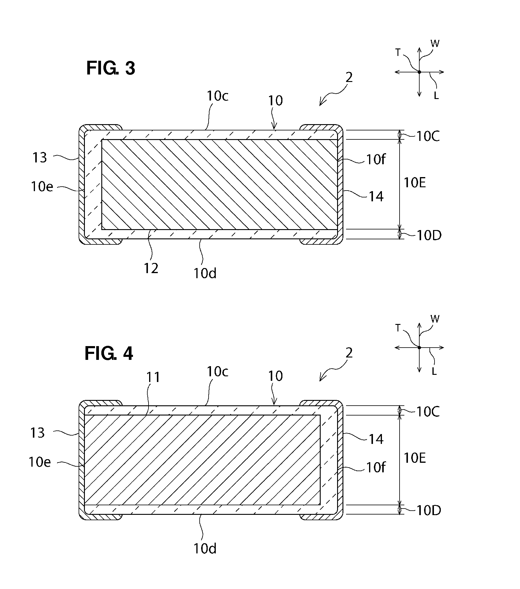
[0044]FIG. 1 is a schematic perspective view of a ceramic electronic component according to a first preferred embodiment of the present invention. FIG. 2 is a cross-sectional view taken along the line II-II in FIG. 1. FIG. 3 is a schematic cross-sectional view taken along the line III-III in FIG. 2. FIG. 4 is a schematic cross-sectional view taken along the line IV-IV in FIG. 2. FIG. 5 is a partially enlarged cross-sectional view taken along the line V-V in FIG. 1. FIG. 6 is a schematic enlarged cross-sectional view of a portion VI in FIG. 5.

[0045]As illustrated in FIG. 1, a multilayer ceramic electronic component 2 according to the present preferred embodiment preferably includes a ceramic sintered body 10 having a substantially rectangular parallelepiped shape. The ceramic sintered body 10 includes first and second major surfaces 10a and 10b (first and second surfaces), first and second side surfaces 10c and 10d (third and fourth surfaces), and first and second end surfaces 10e an...

experimental example

[0071]The multilayer ceramic electronic component 2 according to the above-described preferred embodiment was produced and evaluated. As the multilayer ceramic electronic component, a multilayer ceramic capacitor was produced under the conditions described below.

[0072]Preferably, the dimension in the longitudinal direction is about 1.02 mm, the dimension in the width direction is about 0.53 mm, the dimension in the thickness direction is about 0.53 mm, the width of the side gap is about 0.05 mm, and the dimension of the end gap is about 0.09 mm, for example. The dimension of the end gap is the dimension between the tip of the internal electrode, that is, the tip of the first or second internal electrode 11 or 12 in the longitudinal direction L and the first or second end surface 10e or 10f to which that tip is not exposed. The thickness of the ceramic layer disposed between the first and second internal electrodes 11 and 12 is preferably about 1.1 μm and the thickness of an external...

embodiment

Modified Example of First Preferred Embodiment

[0088]FIG. 9 is a partially enlarged front view describing a modified example of the multilayer ceramic electronic component 2 according to the first preferred embodiment. In the present modified example, a saddle 11a is formed on the tip of each of the plurality of first internal electrodes 11. The saddle 11a occurs in an internal electrode edge portion at the time of forming an internal electrode by printing of conductive paste.

[0089]The saddle 11a is thicker than a remaining portion 11b of the first internal electrode 11.

[0090]Accordingly, if the saddles 11a overlap each other in the thickness direction, when a green stack is pressed in the thickness direction before firing, adhesion between the ceramic layers on both sides of each of the saddles 11a, that is, the ceramic green sheets may be decreased. The force exerted by the pressing on the portion in which the saddles 11a overlap each other and that on the portion in which no saddl...


PUM

PropertyMeasurementUnit
thicknessaaaaaaaaaa
grain sizeaaaaaaaaaa
thicknessaaaaaaaaaa

Abstract

A multilayer ceramic electronic component that is small, that has high electrical strength, and that is resistant to separation between ceramic layers includes a ceramic sintered body having a substantially rectangular parallelepiped shape and a plurality of first and second internal electrodes. The plurality of first and second internal electrodes are alternately arranged so as to face each other. The first and second internal electrodes are parallel or substantially parallel to first and second major surfaces. The first and second internal electrodes are exposed to at least one of the fifth and sixth surfaces and are not exposed to the third or fourth surface. No bends exist in any of the ends of each of the first and second internal electrodes adjacent to the third and fourth surfaces.

Description

BACKGROUND OF THE INVENTION[0001]1. Field of the Invention[0002]The present invention relates to a multilayer ceramic electronic component. In particular, the present invention relates to a multilayer ceramic electronic component that includes a ceramic sintered body having a substantially rectangular parallelepiped shape and a plurality of first and second internal electrodes alternately arranged in the ceramic sintered body so as to face each other.[0003]2. Description of the Related Art[0004]In electronic devices, such as cellular phones and notebook computers, multilayer ceramic electronic components, typified by, for example, multilayer ceramic capacitors, have been frequently used.[0005]In recent years, multilayer ceramic capacitors have become smaller and smaller and their capacities have become larger and larger. A large-capacity multilayer ceramic capacitor of 10 μF to 100 μF is used in a power supply circuit or other circuit, in which an aluminum electrolytic capacitor or ...

Claims


Application Information

Patent Timeline
Patent Type & Authority Applications(United States)
IPC IPC(8): H01G4/12
CPCH01G4/005H01G4/01H01G4/232H01G4/228H01G4/30H01G4/12
Inventor YAMASHITA, YASUHARUOKAJIMA, KENICHITANAKA, HIDEAKIMURANISHI, NAOTOFUKUNAGA, DAIKIOMORI, NAGATO
Owner MURATA MFG CO LTD
Why Eureka
Try Eureka