Light-Emitting Device, Electronic Appliance, and Lighting Device

a technology of light-emitting devices and lighting devices, which is applied in the direction of light-emitting devices, semiconductor devices for light sources, organic semiconductor devices, etc., can solve the problems of increasing the number of masks, the difficulty of adjusting the distance between the electrodes, and the color purity of some pixels, so as to achieve high light-extraction efficiency, cost reduction, and favorable color purity

Active Publication Date: 2012-10-11
SEMICON ENERGY LAB CO LTD
View PDF5 Cites 31 Cited by
  • Summary
  • Abstract
  • Description
  • Claims
  • Application Information

AI Technical Summary

Benefits of technology

[0009]Light-emitting elements utilizing a microcavity system are advantageous for full color display. For example, unlike light-emitting elements which are separately formed depending on the colors R, G, and B, the light-emitting elements utilizing a microcavity system do not need to be separately formed depending on the colors R, G, and B; thus, higher definition can be easily achieved. As compared with a light-emitting element using a color filter (CF) system, the light-emitting elements utilizing a microcavity system can have low power consumption.
[0011]Thus, according to one embodiment of the present invention, a light-emitting device and a lighting device each of which includes a plurality of light-emitting elements exhibiting light with different wavelengths and utilizes a microcavity system are provided. The light-emitting device and the lighting device each have an element structure in which only light with a desired wavelength is emitted from each of the light-emitting elements, and thus the light-emitting elements have favorable color purity and high light-extraction efficiency. Moreover, the number of steps and the cost are reduced.
[0024]According to one embodiment of the present invention, a light-emitting device and a lighting device each of which includes a plurality of light-emitting elements exhibiting light with different wavelengths and utilizes a microcavity system can be provided. The light-emitting device and the lighting device each have an element structure in which light with a desired wavelength is emitted from each of the light-emitting elements by setting the optical path length from a reflective electrode to a light-emitting layer (a light-emitting region) and the optical path length from the reflective electrode to a semi-transmissive and semi-reflective electrode to the predetermined values. Thus, the light-emitting elements can have favorable color purity and high light-extraction efficiency. Further, according to one embodiment of the present invention, a transparent conductive layer does not need to be formed in a light-emitting element from which light with the longest wavelength is extracted; accordingly, the number of steps and the cost can be reduced.

Problems solved by technology

However, there is a problem in that color purity is decreased in some pixels in which a plurality of wavelengths coexists.
There is also a problem of an increase in the number of masks and steps needed for the adjustment of the distance between the pair of electrodes.

Method used


Image

  • Light-Emitting Device, Electronic Appliance, and Lighting Device
  • Light-Emitting Device, Electronic Appliance, and Lighting Device
  • Light-Emitting Device, Electronic Appliance, and Lighting Device

Examples


embodiment 1

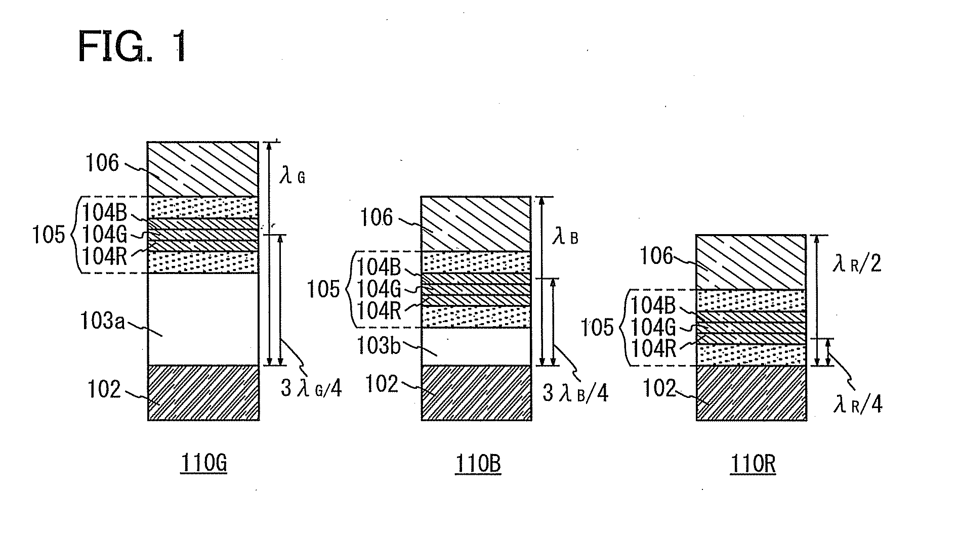
[0035]In this embodiment, a light-emitting device according to one embodiment of the present invention will be described with reference to FIG. 1. Note that hereinafter, an optical path length represents the thickness of a component.

[0036]As illustrated in FIG. 1, the light-emitting device according to one embodiment of the present invention includes light-emitting elements (a first light-emitting element (G) 110G, a second light-emitting element (B) 110B, and a third light-emitting element (R) 110R) having different structures.

[0037]The first light-emitting element (G) 110G has a structure in which a first transparent conductive layer 103a; an EL layer 105 including a first light-emitting layer (R) 104R, a second light-emitting layer (G) 104G, and a third light-emitting layer (B) 104B in part; and a semi-transmissive and semi-reflective electrode 106 are sequentially stacked over a reflective electrode 102. The second light-emitting element (B) 110B has a structure in which a secon...

embodiment 2

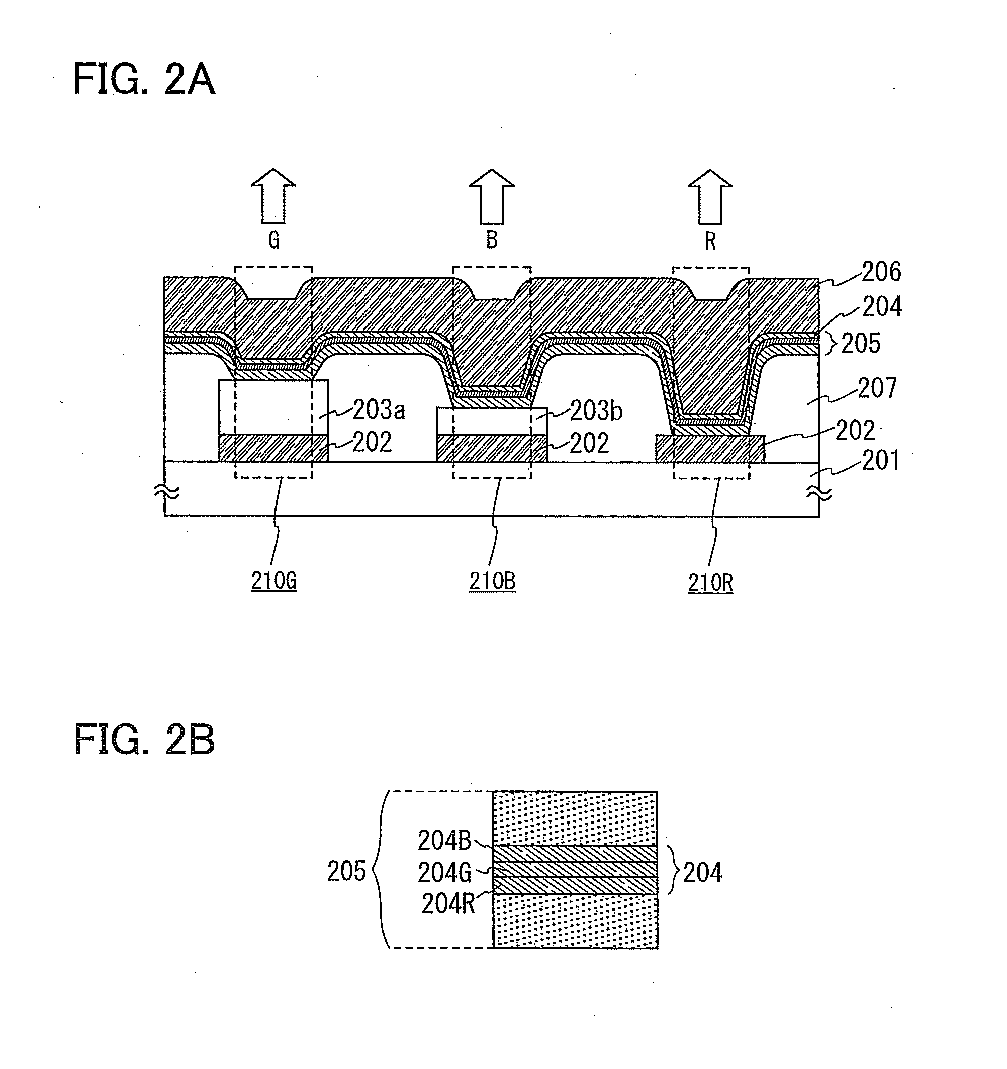
[0052]In this embodiment, a specific structure of the light-emitting device according to one embodiment of the present invention, which is described in Embodiment 1, will be described with reference to FIGS. 2A and 2B.

[0053]A light-emitting device described in this embodiment includes a first light-emitting element (G) 210G in which a reflective electrode 202, a first transparent conductive layer 203a, an EL layer 205 including a light-emitting layer 204, and a semi-transmissive and semi-reflective electrode 206 are sequentially stacked over a substrate 201; a second light-emitting element (B) 210B in which the reflective electrode 202, a second transparent conductive layer 203b, the EL layer 205 including the light-emitting layer 204, and the semi-transmissive and semi-reflective electrode 206 are sequentially stacked over the substrate 201; and a third light-emitting element (R) 210R in which the reflective electrode 202, the EL layer 205 including the light-emitting layer 204, an...

embodiment 3

[0097]In this embodiment, a structure of a light-emitting element included in a light-emitting device according to one embodiment of the present invention will be described with reference to FIG. 3. Note that hereinafter, an optical path length represents the thickness of a component.

[0098]As illustrated in FIG. 3, the light-emitting device according to one embodiment of the present invention includes light-emitting elements (a first light-emitting element (G) 310G, a second light-emitting element (B) 310B, and a third light-emitting element (R) 310R) having different structures.

[0099]The first light-emitting element (G) 310G has a structure in which a first transparent conductive layer 303a; an EL layer 305 including a first light-emitting layer (Y) 304Y and a second light-emitting layer (B) 304B in part; and a semi-transmissive and semi-reflective electrode 306 are sequentially stacked over a reflective electrode 302. The second light-emitting element (B) 310B has a structure in w...


PUM


Abstract

A light-emitting device and a lighting device each of which includes a plurality of light-emitting elements exhibiting light with different wavelengths are provided. The light-emitting device and the lighting device each have an element structure in which each of the light-emitting elements emits only light with a desired wavelength, and thus the light-emitting elements have favorable color purity. In the light-emitting element emitting light (λR) with the longest wavelength of the light with different wavelengths, the optical path length from a reflective electrode to a light-emitting layer (a light-emitting region) included in an EL layer is set to λR / 4 and the optical path length from the reflective electrode to a semi-transmissive and semi-reflective electrode is set to λR / 2.

Description

BACKGROUND OF THE INVENTION[0001]1. Field of the Invention[0002]The present invention relates to a light-emitting device and a lighting device which utilize electroluminescence.[0003]2. Description of the Related Art[0004]In recent years, research and development have been extensively conducted on light-emitting elements utilizing electroluminescence (EL). In a basic structure of such a light-emitting element, a layer containing a light-emitting substance (an EL layer) is interposed between a pair of electrodes. By voltage application to this element, light emission can be obtained from the light-emitting substance.[0005]Since such a light-emitting element is of self-light-emitting type, it is considered that the light-emitting element has advantages over a liquid crystal display, such as high pixel visibility and the eliminated need for a backlight. Accordingly, such a light-emitting element is thought to be suitable as a flat panel display element. Such a light-emitting element is...

Claims


Application Information

Patent Timeline
Patent Type & Authority Applications(United States)
IPC IPC(8): H01L33/60
CPCH01L51/504H01L2251/558H01L27/3211H01L51/5265F21K9/00H01L33/36H10K50/125H10K50/80H10K2102/301H10K59/35H10K50/13H10K50/852H10K2102/351H10K50/11H10K50/15H10K50/16H10K50/17H10K50/171H10K50/818H10K50/828
Inventor HATANO, KAORU
Owner SEMICON ENERGY LAB CO LTD
Why Eureka
Try Eureka