Solid-state imaging device and method for manufacturing the same

a solid-state imaging and imaging device technology, applied in the direction of radio frequency controlled devices, instruments, lenses, etc., can solve the problems of color mixture, difficult for light whose propagation direction is changed at the upper surface of the color filter to leak into an adjacent pixel portion, and the above-mentioned problem is further noticeabl

Active Publication Date: 2012-10-25
PANASONIC SEMICON SOLUTIONS CO LTD
View PDF5 Cites 33 Cited by
  • Summary
  • Abstract
  • Description
  • Claims
  • Application Information

AI Technical Summary

Benefits of technology

[0030]In the method for manufacturing a solid-state imaging device according to the present invention, it is possible to adopt a structure in which lower surfaces of the color filters in the direction of lamination are also arranged in a concave shape in the step of forming the color filters. With this structure, the lower surfaces of the color filters also have a concave shape, which is excellent in view of collecting light.
[0031]It should be noted that the foregoing effects can be obtained when the color filter has a refraction index that is higher than a refraction index of a portion of the wiring layer located under the color filter, which makes contact with the lower surface of the color filter. Contrary to this, if the relation of the two refraction indices is reversed, a similar effect can be obtained by arranging the lower surface of the color filter in a convex shape.
[0032]In the method for manufacturing a solid-state imaging device according to the present invention, a step of forming, on the wiring layer, partition walls in a grid pattern with openings provided in positions individually corresponding to above the plurality of light-receiving portions subsequent to the step of forming the wiring layer but prior to the step of forming the plurality of color filters. Then, it is possible to adopt a structure in which, in the step of forming the plurality of color filters, each of the color filters is formed in each of the openings opened in each of the partition walls. With this structure, adjacent color filters are divided by the partition wall, and it is therefore possible to manufacture a solid-state imaging device excellent in preventing light from penetrating into an adjacent pixel portion.
[0033]In the method for manufacturing a solid-state imaging device according to the present invention, it is possible to adopt a structure in which, in the step of forming the wiring layer, recesses are provided in positions individually corresponding to above the plurality of light-receiving portions. Further, it is also possible to adopt a structure in which, subsequent to the step of forming the wiring layer but prior to the step of forming the plurality of color filters, there is provided a step of burying a second insulating film having a refraction index higher than a refraction index of the insulating film of the wiring layer inside each of the recesses. With this structure, it is possible to manufacture a solid-state imaging device in which the second insulating film serves as a core portion of a light waveguide, and collected light is prevented from leaking into the insulating film of the wiring layer but can be reliably guided to the light-receiving portion.

Problems solved by technology

However, according to the solid-state imaging device proposed in Unexamined Japanese Patent Publication No. 1103-282403, there is a case in which light propagating obliquely after passing through a microlens enters an adjacent pixel portion and causes a problem of color mixture.
This makes the above-mentioned problem further noticeable.
This structure makes it difficult for light whose propagation direction is changed at the upper surface of the color filter to leak into an adjacent pixel portion.

Method used


Image

  • Solid-state imaging device and method for manufacturing the same
  • Solid-state imaging device and method for manufacturing the same
  • Solid-state imaging device and method for manufacturing the same

Examples


first exemplary embodiment

1. Overall Configuration of Solid-State Imaging Device 1

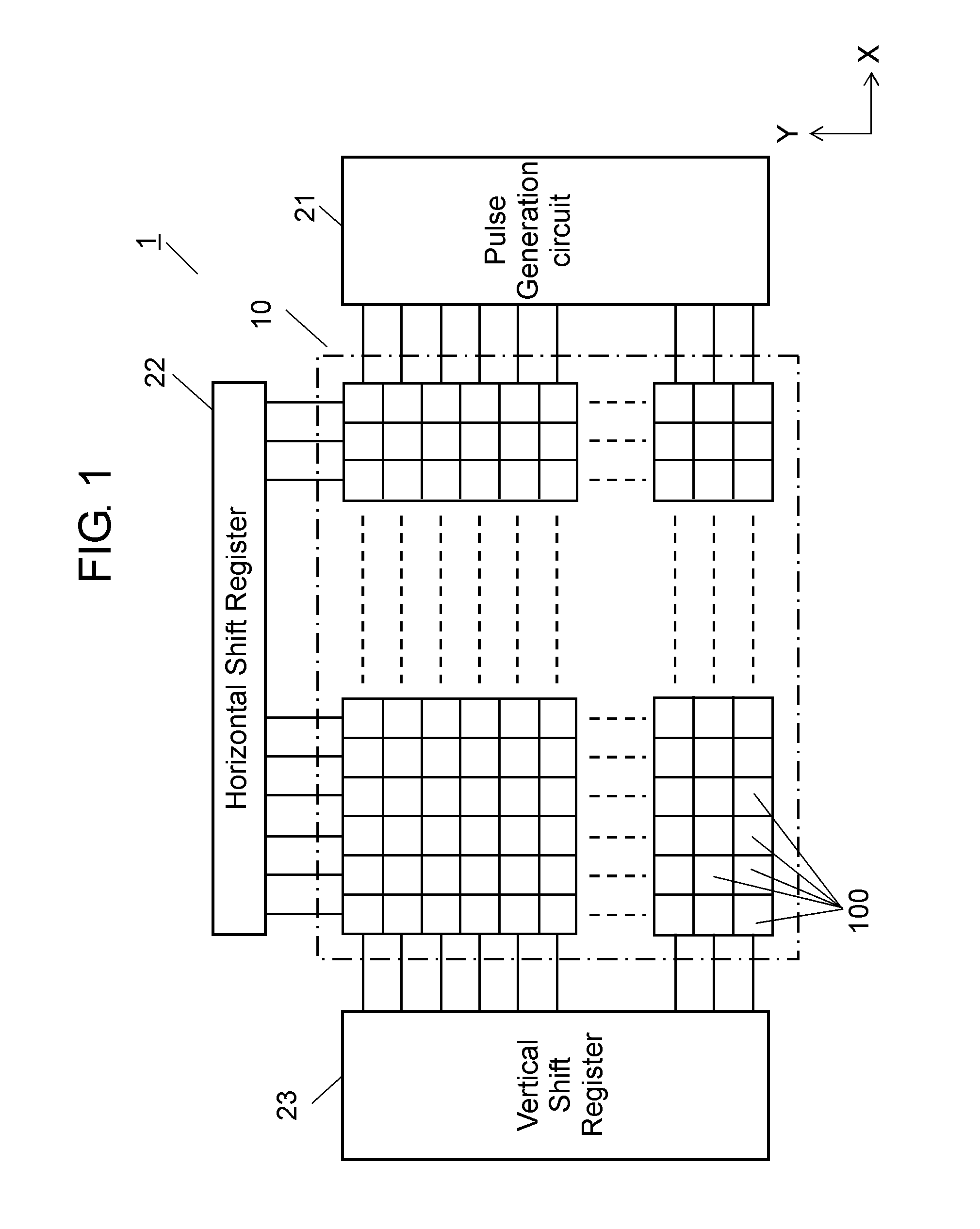
[0050]An overall configuration of solid-state imaging device 1 according to the first exemplary embodiment will be described with reference to FIG. 1.

[0051]As illustrated in FIG. 1, in solid-state imaging device 1 according to the first exemplary embodiment, a plurality of pixel portions 100 are arranged in a matrix form along an X-Y plane to thereby form pixel region 10. Pulse generation circuit 21, horizontal shift register 22, and vertical shift register 23, which are arranged on a periphery of pixel region 10 are connected to pixel region 10. Horizontal shift register 22 and vertical shift register 23 sequentially output driving pulses to each of pixel portions 100 in response to a timing pulse from pulse generation circuit 21.

2. Structure of Pixel Portions 100 of Solid-State Imaging Device 1

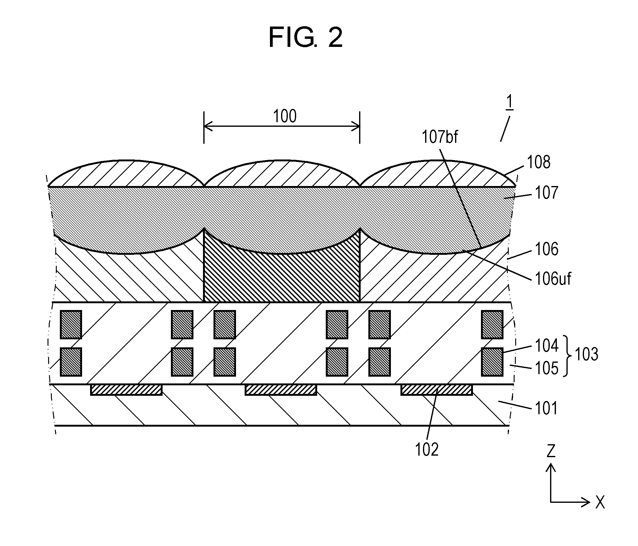
[0052]Structure of pixel portions 100 of solid-state imaging device 1 will be described with reference to FIG. 2.

[0053]As illustrated ...

second exemplary embodiment

[0078]A structure of solid-state imaging device 2 according to a second exemplary embodiment will be described with reference to FIG. 7. FIG. 7 illustrates a part of pixel portions 200 in a pixel region taken out from the structure of solid-state imaging device 2, and structures other than that of the pixel region are the same as those in the first exemplary embodiment. Also, in the description hereinafter, descriptions of the structures similar to those of the first exemplary embodiment will not be repeated.

[0079]As illustrated in FIG. 7, in solid-state imaging device 2 according to this exemplary embodiment, partition walls 209 are interposed between color filters 206 of adjacent pixel portions 200. Then, color filters 206 are individually formed between adjacent partition walls 209, and upper surfaces 206uf of the color filters 206 have a concave shape as in the case of the first exemplary embodiment.

[0080]Planarized film 207 on color filter 206 has its lower surface 207bf making...

third exemplary embodiment

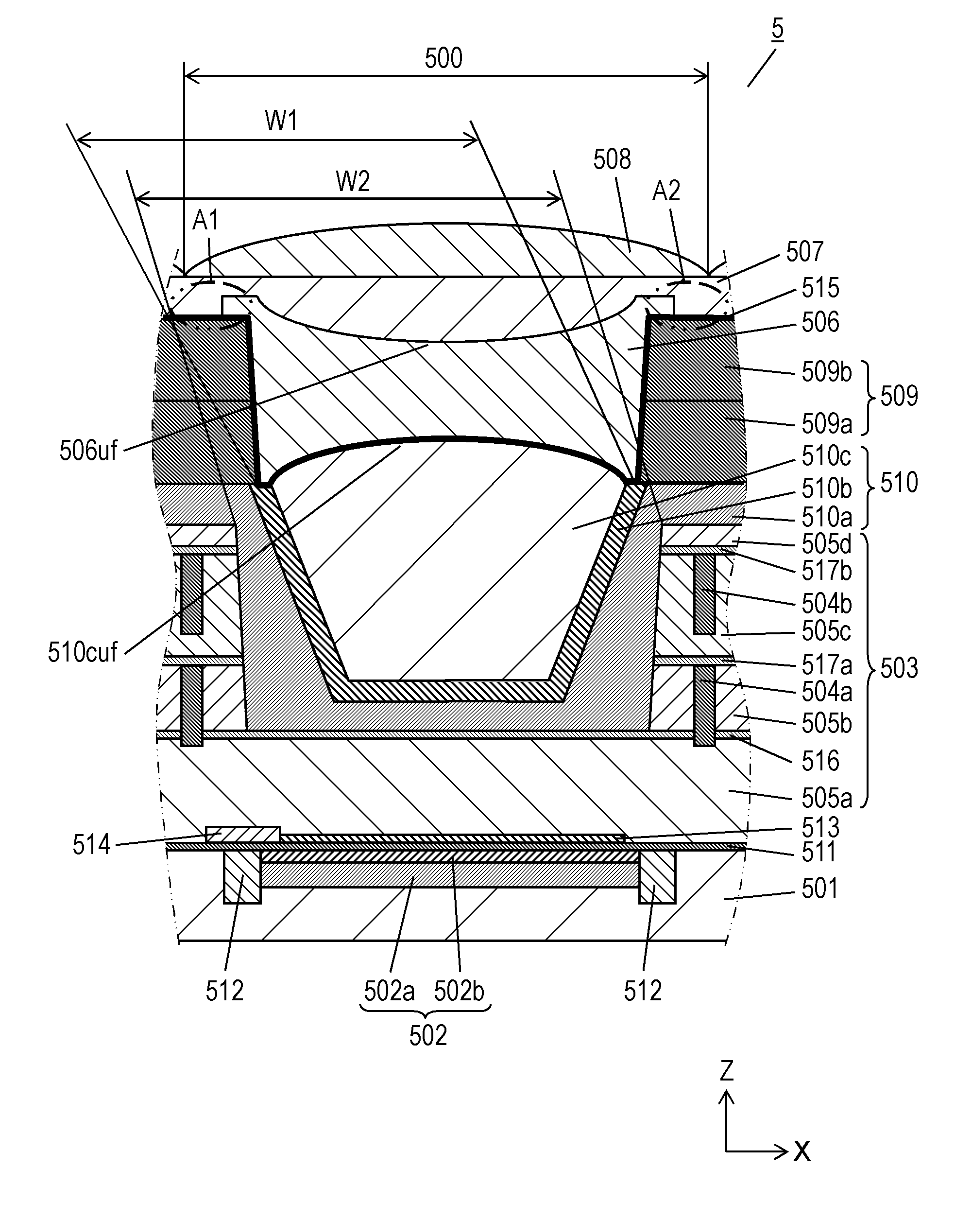
[0086]A structure of solid-state imaging device 3 according to a third exemplary embodiment will be described with reference to FIG. 8. FIG. 8 illustrates a part of pixel portions 300 in a pixel region taken out from the structure of solid-state imaging device 3, and structures other than that of the pixel region are the same as those in the first and second exemplary embodiments. Also, in the description hereinafter, descriptions of the structures similar to those of the first and second exemplary embodiments will not be repeated.

[0087]As illustrated in FIG. 8, in solid-state imaging device 3 according to this exemplary embodiment, a recess is formed in insulating film 305 of wiring layer 303 at a position above photodiode 102 in each of pixel portions 300. Then, insulating film (core portion) 310 is buried in the recess opened in insulating film 305 of wiring layer 303. Core portion 310 is formed of, for example, silicon nitride (SiN) and has a refraction index of about 1.9 to 2.0...


PUM


Abstract

A solid-state imaging device and a method for manufacturing the same are provided. The solid-state imaging device includes a structure that provides a high sensitivity and high resolution without variations in spectral sensitivity and without halation of colors, and prevents light from penetrating into an adjacent pixel portion. A plurality of photodiodes are formed inside a semiconductor substrate. A wiring layer includes a laminated structure of an insulating film and a wire and is formed on the semiconductor substrate. A plurality of color filters are formed individually in a manner corresponding to the plurality of photodiodes above the wiring layer. A planarized film and a microlens are sequentially laminated on each of the color filters. In the solid-state imaging device, each of the color filters has an refraction index higher than that of the planarized film and has, in a Z-axis direction, an upper surface in a concave shape.

Description

BACKGROUND[0001]1. Technical Field[0002]The present invention relates to a solid-state imaging device and a method for manufacturing the same, and more particularly to a structure of color filters.[0003]2. Background Art[0004]A solid-state imaging device is used as an imaging device for a digital still camera, a video camera, or the like. The solid-state imaging device has a structure in which, for example, a plurality of photodiodes (light-receiving portions) is formed in a surface layer of one side of a semiconductor substrate, and each of the photodiodes performs photoelectric conversion and outputs image signals. Here, each of color filters for colors of red (R), green (G), and blue (B) is formed above each of the photodiodes, and therefore light having a light component of a wavelength band selected when the light passes through each of the color filters enters each of the photodiodes. As an example, a structure of a solid-state imaging device disclosed in Unexamined Japanese P...

Claims


Application Information

Patent Timeline
Patent Type & Authority Applications(United States)
IPC IPC(8): H01L27/146H01L31/0232H01L31/18
CPCH01L27/14621H01L27/14627G02B5/201H01L27/14687G02B3/0056H01L27/14629
Inventor NAKAMURA, TETSUYAKATSUNO, MOTONARITAKASE, MASAYUKIKATAOKA, MASAO
Owner PANASONIC SEMICON SOLUTIONS CO LTD
Why Eureka
Try Eureka