Sheet for protecting surface of semiconductor wafer, semiconductor device manufacturing method and semiconductor wafer protection method using sheet
Active Publication Date: 2012-11-01
MITSUI CHEM TOHCELLO INC
View PDF10 Cites 20 Cited by
Summary
Abstract
Description
Claims
Application Information
AI Technical Summary
This helps you quickly interpret patents by identifying the three key elements:
Problems solved by technology
Method used
Benefits of technology
Benefits of technology
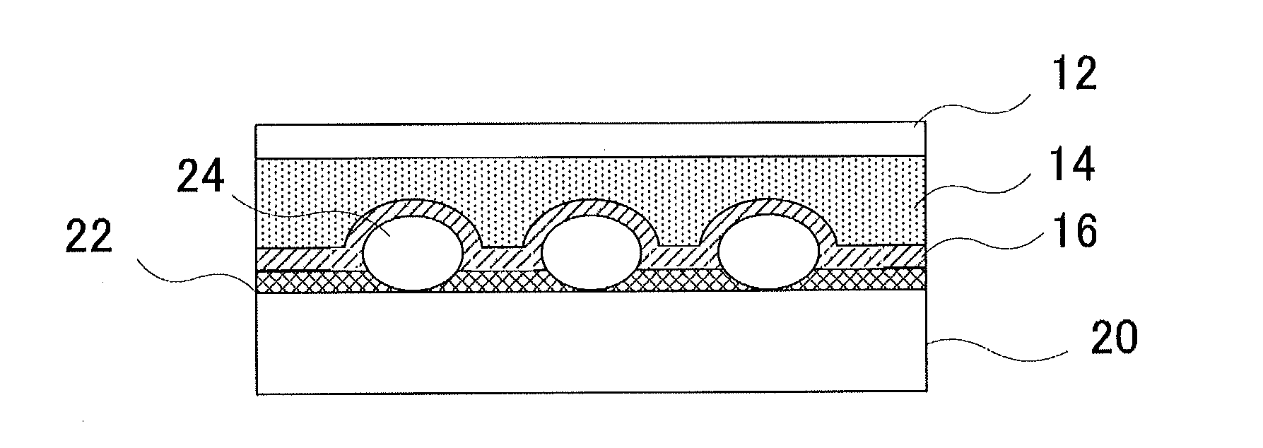
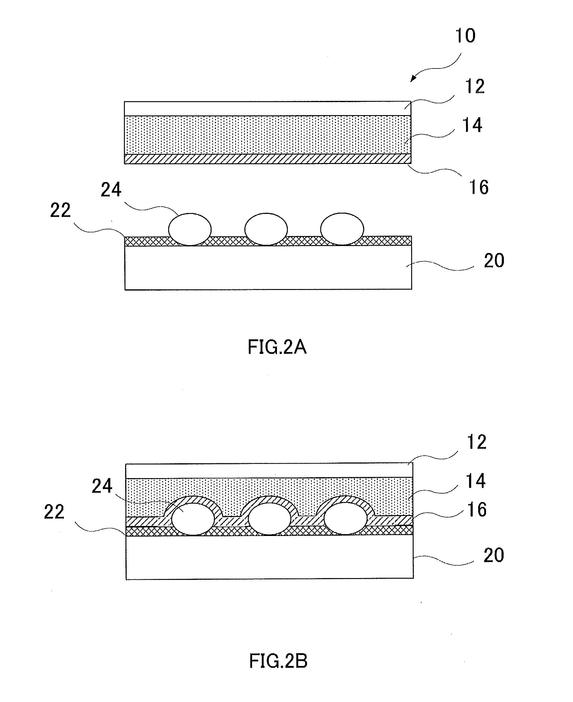
[0011]The present invention has been made in view of the foregoing circumstances. An object of the present invention is to provide a semiconductor wafer surface protection sheet that has good adhesion to irregularities on a patterned surface of a semiconductor wafer and has good peelability after grinding, and a method of protecting a semiconductor wafer using the semiconductor wafer surface protection sheet. Another object of the present invention is to provide a semiconductor wafer surface protection sheet that may have good peelability even from a porous circuit protection layer or from a patterned surface with complex irregularities.
Problems solved by technology
Thus, when attaching a semiconductor wafer surface protection sheet to the semiconductor wafer, creation of voids between the semiconductor wafer surface protection sheet and the irregularity on the patterned surface of the semiconductor wafer results in a uneven distribution of stress across the surface of the semiconductor wafer upon grinding of its non-patterned surface, making the semiconductor wafer liable to breakage.
Method used
Image
Click on the blue label to locate the original text in one second.
Reading with bidirectional positioning of images and text.
Examples
examples 1 and 2
[0090]1. Measurement of Tensile Elasticity of Respective Layers
[0091]As a base film, a polyethylene terephthalate film (thickness: 75 μm) is provided. As a film for resin layer A, a 100 μm-thick film is provided which is obtained by extrusion molding of TAFMER P0275® (Mitsui Chemicals, Inc., density=861 kg / m3). As a film for resin layer B, a 100 μm-thick film is provided which is obtained by extrusion molding of Notio PN 3560 manufactured by Mitsui Chemicals, Inc. Tensile elasticity is measured for these films in the procedure described below.
[0092]The films are each cut into a piece with an initial dimension of 14 cm length and 1 cm width to prepare sample films for measurement. Tensile test is then conducted under the following conditions to measure elongation (mm) of the sample film: measurement temperature =25 C°, distance between chucks=100 mm, and tensile speed=50 mm / min. A tangent line is drawn to the initial rising section of the obtained stress-strain curve (S-S curve), and...
examples 3 and 4
[0109]Instead of the semiconductor wafer prepared in Example 1, semiconductor wafers having a porous circuit protection layer formed on the patterned surface are provided. The porous circuit protection layer is prepared in the procedure described below.
[0110]1) Synthesis of Polyhydroxyamide (Polybenzooxazol Precursor)
[0111]27.0 g (0.2 mol) of 1-hydroxybenzotriazol (KUROGANE KASEI Co., Ltd., HBT) is dissolved in 150 mL of N,N-dimethylacetylacetamide (Wako Pure Chem Industries, Ltd., DMAc), and the solution is cooled to −10 C°. 20.2 g (0.2 mol) of triethylamine (Wako Pure Chem Industries, Ltd.) is added to the solution.
[0112]29.5 g (0.1 mol) of 4,4′-dicarbonylchloride diphenyl ether (NIHON NOHYAKU Co., Ltd., DEC) is dissolved in 150 mL of acetone, after which this solution: is added dropwise to the above-prepared mixture solution of HBT, DMAc and triethylamine while keeping the liquid temperature below 0 C°. The solution is stirred for 2 hours at −10 C°, warmed to room temperature, an...
example 5
[0123]A semiconductor wafer surface protection sheet is obtained in the same manner as in Example 1 except that the thickness of resin layer B is changed to 20 μm. Evaluations for the semiconductor wafer surface protection sheet and a wafer after grinding are made in the same manner as in Example 3.
PUM
Property
Measurement
Unit
Temperature
aaaaa
aaaaa
Temperature
aaaaa
aaaaa
Temperature
aaaaa
aaaaa
Abstract
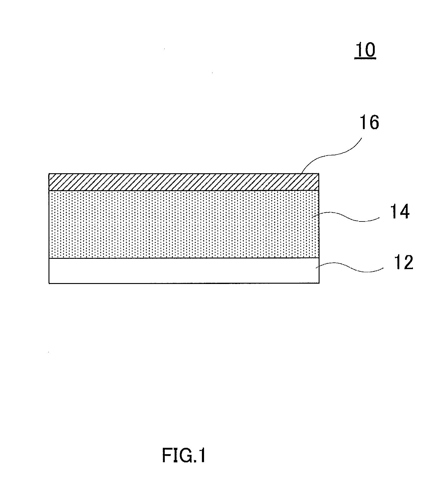
To provide a semiconductorwafer surface protection sheet having good adhesion to irregularities on a patterned surface of a semiconductorwafer and having good peelability after wafergrinding. Specifically, a semiconductor wafer surface protection sheet is provided that includes a base layer having a tensile elasticity at 25 C°, E(25), of 1 GPa or more; a resin layer A that satisfies the condition EA(60) / EA(25) <0.1, where EA(25) is a tensile elasticity at 2 C° and EA(60) is a tensile elasticity at 60° C., the EA(60) ranging from 0.005 MPa to 1 MPa; and a resin layer B having a tensile elasticity at 60° C., EB(60), of 1 MPa or more and having a thickness of 0.1 μm to less than 100 μm, the EB(60) being larger than the EA(60) of the resin layer A.
Description
TECHNICAL FIELD[0001]The present invention relates to a semiconductor wafer surface protection sheet, a method of protecting a semiconductor wafer using the same, and a method of manufacturing a semiconductor device using the same.BACKGROUND ART[0002]During the grinding step of the non-patterned surface of a semiconductor wafer in a manufacturing process of semiconductor devices from a semiconductor wafer, a semiconductor wafer surface protection sheet is attached to the patterned surface of the semiconductor wafer in order to prevent possible damage to the patterned surface.[0003]The patterned surface of a semiconductor wafer has irregularities that include not only circuits, but also relatively high differences in level such as semiconductor bumps. Thus, when attaching a semiconductor wafer surface protection sheet to the semiconductor wafer, creation of voids between the semiconductor wafer surface protection sheet and the irregularity on the patterned surface of the semiconducto...
Claims
Application Information
Patent Timeline
Application Date:The date an application was filed.
Publication Date:The date a patent or application was officially published.
First Publication Date:The earliest publication date of a patent with the same application number.
Issue Date:Publication date of the patent grant document.
PCT Entry Date:The Entry date of PCT National Phase.
Estimated Expiry Date:The statutory expiry date of a patent right according to the Patent Law, and it is the longest term of protection that the patent right can achieve without the termination of the patent right due to other reasons(Term extension factor has been taken into account ).
Invalid Date:Actual expiry date is based on effective date or publication date of legal transaction data of invalid patent.

