Quantum dot channel (QDC) quantum dot gate transistors, memories and other devices

a quantum dot gate transistor and quantum dot channel technology, applied in the field of field-effect transistors, can solve the problems of limited current fets, limited current fet functionality, and limited applications for current transistors

Active Publication Date: 2012-11-08
JAIN FAQUIR CHAND
View PDF6 Cites 62 Cited by
  • Summary
  • Abstract
  • Description
  • Claims
  • Application Information

AI Technical Summary

Problems solved by technology

Unfortunately however, current FETs have only one inversion layer which is formed in the proximity of the gate insulator.
Thus, the applications for current transistors are limited in that designs must take into account the bi-state functionality of the FETs.
Accordingly, functionality of current FETs are limited.

Method used


Image

  • Quantum dot channel (QDC) quantum dot gate transistors, memories and other devices
  • Quantum dot channel (QDC) quantum dot gate transistors, memories and other devices
  • Quantum dot channel (QDC) quantum dot gate transistors, memories and other devices

Examples


Embodiment Construction

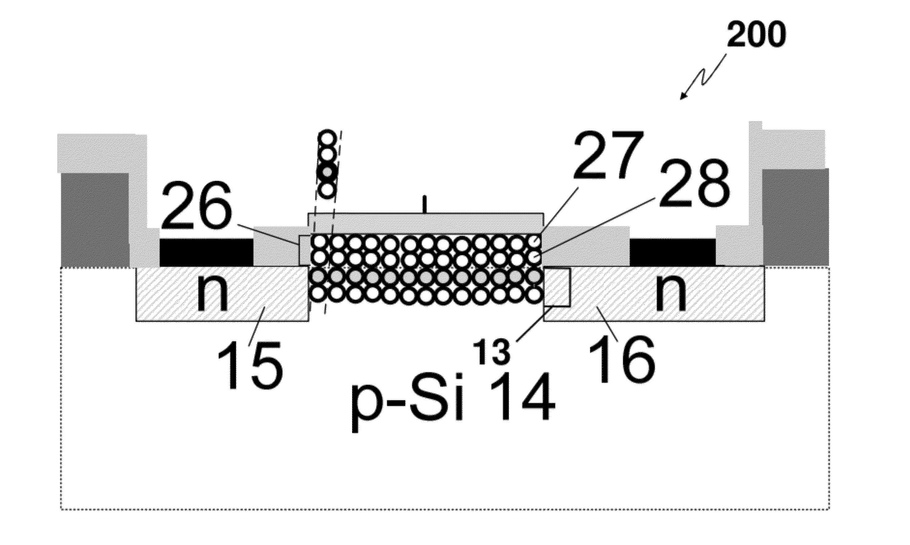
[0049]In accordance with the invention, a field-effect transistor in which a channel is formed in an array of quantum dots is provided and described herein. In one embodiment the quantum dots are cladded with a thin layer serving as an energy barrier. The array of quantum dots with a thin barrier (about 1-2 nm) form a superlattice like layer in two or three dimensions. The quantum dot channel (QDC) may consist of one or more layers of cladded quantum dots. These quantum dots may be realized on a single or polycrystalline substrate. It should be appreciated that when QDC FETs are realized on polycrystalline or nanocrystalline thin films, they may yield higher mobility than in conventional nano- or microcrystalline thin films. These FETs can advantageously be used as thin film transistors (TFTs) in a variety of applications. In another embodiment QDC-FETs are combined with: (a) coupled quantum well Spatial Wavefunction Switched (SWS) channels and (b) quantum dot layers like used in 3-...


PUM


Abstract

This invention describes a field-effect transistor in which the channel is formed in an array of quantum dots. In one embodiment the quantum dots are cladded with a thin layer serving as an energy barrier. The quantum dot channel (QDC) may consist of one or more layers of cladded dots. These dots are realized on a single or polycrystalline substrate. When QDC FETs are realized on polycrystalline or nanocrystalline thin films they may yield higher mobility than in conventional nano- or microcrystalline thin films. These FETs can be used as thin film transistors (TFTs) in a variety of applications. In another embodiment QDC-FETs are combined with: (a) coupled quantum well SWS channels, (b) quantum dot gate 3-state like FETs, and (c) quantum dot gate nonvolatile memories.

Description

CROSS REFERENCE TO RELATED APPLICATIONS[0001]This application claims priority to and benefit of the filing date of U.S. Provisional Patent Application No. 61 / 483,553, filed May 6, 2011, the contents of which are incorporated herein by reference in its entirety.STATEMENT REGARDING FEDERALLY SPONSORED RESEARCH[0002]The United States Government has certain rights in this invention pursuant to National Science Foundation Grant No. ECS 0622068.FIELD OF THE INVENTION[0003]The present invention applies to field-effect transistors (FETs) and more particularly to FETs using quantum dot channels, nonvolatile random access memories (RAMs) with addressable quantum dot floating gates and ultrahigh value capacitors for energy storage as well as a method of fabricating heteroepitaxial structures which are mediated by quantum dot layers to reduce defects.BACKGROUND OF THE INVENTION[0004]In the past few years, researchers have investigated various approaches to fabricating FETs which range from usin...

Claims


Application Information

Patent Timeline
Patent Type & Authority Applications(United States)
IPC IPC(8): H01L29/775H01L31/0352
CPCB82Y10/00B82Y20/00H01L21/28273H01L29/0665H01L29/42332H01L29/66825H01L29/7881H01L31/028H01L31/035218H01L31/035236H01L31/078H01L29/125Y02E10/547G11C16/0408B82Y40/00H01L29/40114
Inventor JAIN, FAQUIR CHAND
Owner JAIN FAQUIR CHAND
Why Eureka
Try Eureka