Display device and display array substrate

a display array and substrate technology, applied in static indicating devices, instruments, non-linear optics, etc., can solve the problems of reducing yield and esd damage of lcd devices, and achieve the effect of enhancing esd protection and reducing esd damage for ic and other lines

Active Publication Date: 2012-11-08
E INK HLDG INC
View PDF8 Cites 15 Cited by
  • Summary
  • Abstract
  • Description
  • Claims
  • Application Information

AI Technical Summary

Benefits of technology

[0013]The display device and the display array substrate of the exemplary embodiment of the present invention dispose the conductive loop in the periphery region of the display array substrate, and the conductive loop passes through the chip-bonding area, to conduct the electro-static charges accumulated somewhere of the display array substrate to the whole display array substrate. Thus the electro-static charges may be uniformly distributed in the whole display array substrate, to reduce the ESD damage for IC and other lines of the display array substrate. In addition, the conductive loop may be further electrically coupled to the common-electrode substrate, for further conducting the electro-static charges to the common electrode which may be an unbroken piece, to further enhance the ESD protection.

Problems solved by technology

The ESD damage of the LCD device generally takes place in the manufacturing process of the LCD device, such as an array manufacturing period, a cell manufacturing period and a module manufacturing period, etc.
However, it only may use machine tables or operation people to reduce the ESD damage in the module manufacturing period.
Thus, the ESD damage often take places in IC pads or between two ICs during the module manufacturing period, and it will reduce the yield thereof.

Method used


Image

  • Display device and display array substrate
  • Display device and display array substrate
  • Display device and display array substrate

Examples


Embodiment Construction

[0020]The present invention will now be described more specifically with reference to the following embodiments. It is to be noted that the following descriptions of preferred embodiments of this invention are presented herein for purpose of illustration and description only. It is not intended to be exhaustive or to be limited to the precise form disclosed.

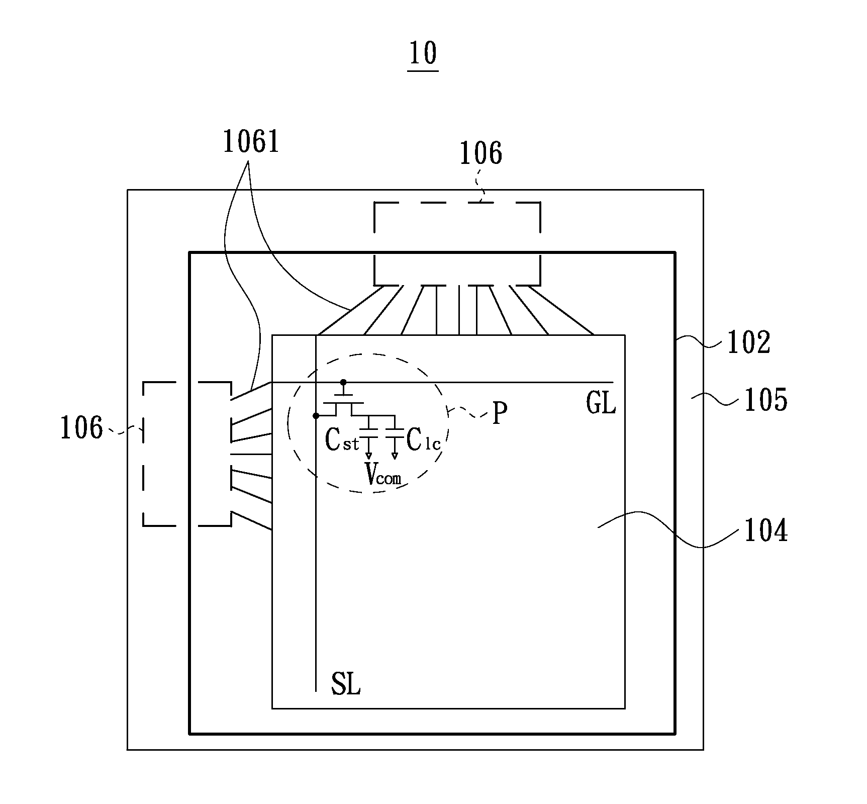
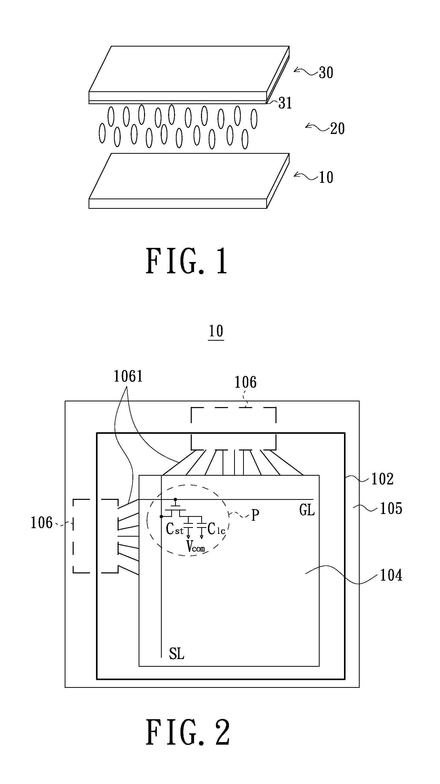
[0021]FIG. 1 is an exploded schematic view of a liquid crystal display (LCD) device in accordance with an exemplary embodiment of the present invention. Referring to FIG. 1, the LCD device includes a display array substrate 10 (also called as a thin-film transistor (TFT) array substrate), a common-electrode substrate 30 opposite to the display array substrate 10, and a liquid crystal display layer 20 sandwiched between the display array substrate 10 and the common-electrode substrate 30. A common electrode 31 is formed on a side of the common-electrode substrate 30 adjacent to the liquid crystal display layer 20. The common elect...


PUM

PropertyMeasurementUnit
chip-bonding aaaaaaaaaa
conductiveaaaaaaaaaa
storage capacitanceaaaaaaaaaa

Abstract

A display device comprises a display array substrate, a common substrate and a display layer. The display array substrate comprises a display region and a periphery region, and at least one chip-bonding area is formed in the periphery region. The display layer is sandwiched between the display array substrate and the common-electrode substrate. A conductive loop is disposed in the periphery region of the display array substrate, and passes through the chip-bonding area.

Description

FIELD OF THE INVENTION[0001]The present invention relates to the display field, and more particularly to a display device and a display array substrate thereof which can avoid the ESD (electro-static discharge) damage.BACKGROUND OF THE INVENTION[0002]Currently, display device, such as liquid crystal display (LCD) device has many advantages, such as high definition, environmental protection, low power-consumption, little radiation, etc., and it has been a trend of the market. The LCD device generally includes a display array substrate (also called as a thin-film transistor (TFT) array substrate), a common-electrode substrate and a liquid crystal display layer sandwiched between the display array substrate and the common-electrode substrate. The display array substrate includes a plurality of scan lines, a plurality of data lines, a plurality of pixel electrodes and a plurality of pixel transistors, etc., which are manufactured by the semiconductor manufacturing technology. The common...

Claims


Application Information

Patent Timeline
Patent Type & Authority Applications(United States)
IPC IPC(8): G02F1/1333
CPCG02F1/1345G09G2330/06G09G2330/04G09G3/3648
Inventor CHEN, JIA-HUNGCHOU, PEI-JU
Owner E INK HLDG INC
Why Eureka
Try Eureka