Scalable high-bandwidth connectivity

a high-bandwidth, scalable technology, applied in the direction of shielding material radiating elements, instruments, and semiconductor/solid-state device details, etc., can solve the problems of requiring expensive electronics to negotiate, affecting signal quality or integrity, etc., to achieve the effect of facilitating conversion

Active Publication Date: 2012-11-15
MOLEX INC
View PDF13 Cites 119 Cited by
  • Summary
  • Abstract
  • Description
  • Claims
  • Application Information

AI Technical Summary

Benefits of technology

[0005]In one example, an electronic storage device may include a dielectric client substrate, a first data storage unit mounted to the client substrate for storing digital information, and a first client EHF communication unit having a first antenna. The first client communication unit mounted to the client substrate may be in communication with the first data storage unit. This may facilitate converting between an EHF electromagnetic signal containing digital information conducted by the first antenna and a data signal conducted by the first data-storage circuit.

Problems solved by technology

Connector and backplane architectures introduce a variety of impedance discontinuities into the signal path, resulting in a degradation of signal quality or integrity.
Connecting to boards by conventional means, such as signal-carrying mechanical connectors, generally creates discontinuities, requiring expensive electronics to negotiate.
Conventional mechanical connectors may also wear out over time, require precise alignment and manufacturing methods, and are susceptible to mechanical jostling.

Method used


Image

  • Scalable high-bandwidth connectivity
  • Scalable high-bandwidth connectivity
  • Scalable high-bandwidth connectivity

Examples


Embodiment Construction

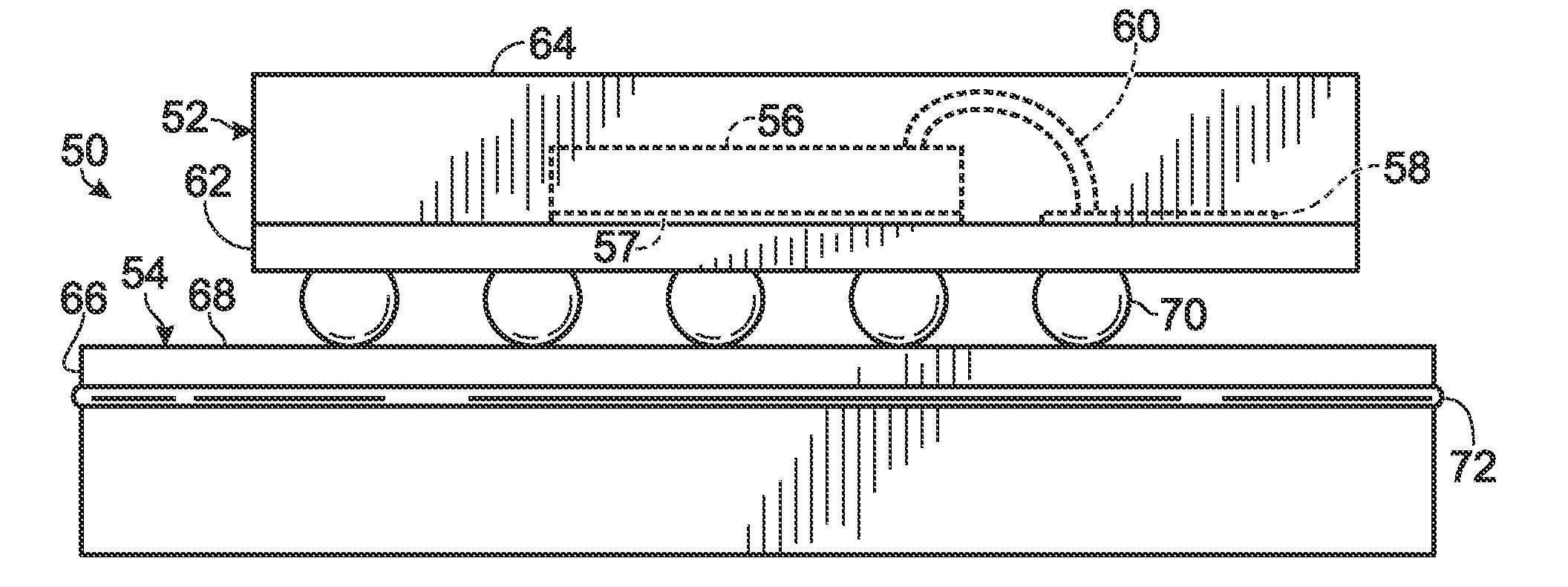
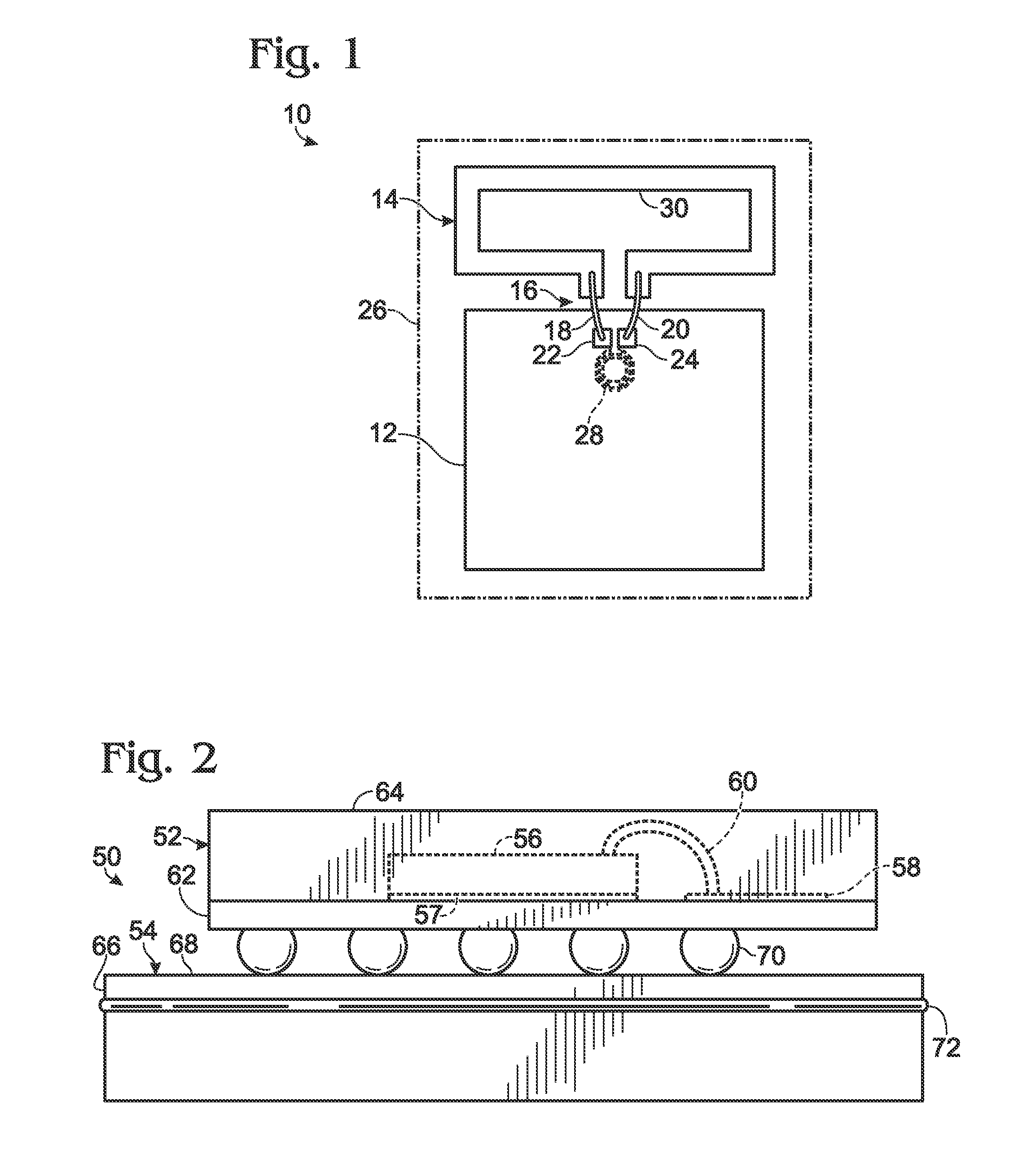
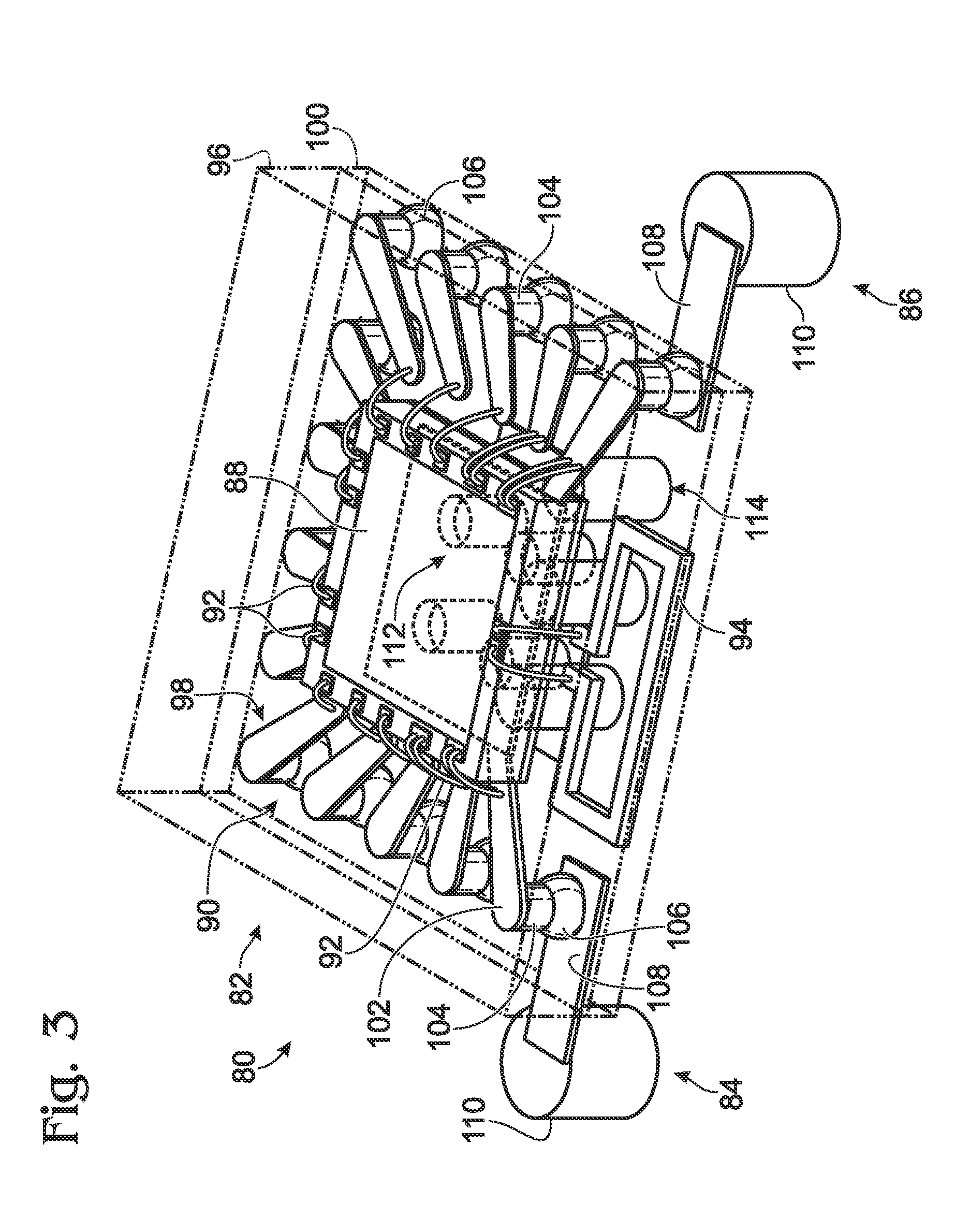
[0037]Wireless communication may be used to provide signal communications between components on a device or may provide communication between devices. Wireless communication provides an interface that is not subject to mechanical and electrical degradation. Examples of systems employing wireless communication between chips are disclosed in U.S. Pat. No. 5,621,913 and U.S. Published Patent Application No. 2010 / 0159829, the disclosures of which are incorporated herein by reference in their entirety for all purposes.

[0038]In one example, tightly-coupled transmitter / receiver pairs may be deployed with a transmitter disposed at a terminal portion of a first conduction path and a receiver disposed at a terminal portion of a second conduction path. The transmitter and receiver may be disposed in close proximity to each other depending on the strength of the transmitted energy, and the first conduction path and the second conduction path may be discontiguous with respect to each other. In s...


PUM


Abstract

A scalable, high-bandwidth connectivity architecture for portable storage devices and memory modules may utilize EHF communication link chip packages mounted in various two-dimensional and three-dimensional configurations on planar surfaces such as printed circuit boards. Multiple electromagnetic communication links between devices distributed on major faces of card-like devices may be provided with respectively aligned pairs of communication units on each device. Adjacent communication units on a printed circuit board may transmit or receive electromagnetic radiation having different polarization, such as linear or elliptical polarization. Power and communication between communication devices may both be provided wirelessly.

Description

CROSS-REFERENCE TO RELATED APPLICATIONS[0001]This application claims the benefit of the following U.S. Provisional patent applications: (i) Ser. No. 61 / 485,543, filed on May 12, 2011 and entitled “Scalable High-Bandwidth Connectivity Method and Apparatus”; (ii) Ser. No. 61 / 535,277, filed on Sep. 15, 2011 and entitled “Wireless Power And Data Transfer System”; and (iii) Ser. No. 61 / 549,378, filed on Oct. 20, 2011 and entitled “Zero Height Connectors”; which applications are incorporated herein by reference in their entirety for all purposes.FIELD OF THE DISCLOSURE[0002]This disclosure relates to systems and methods for EHF communications, including communication associated with modular and portable memory devices.BACKGROUND OF THE DISCLOSURE[0003]Advances in semiconductor manufacturing and circuit design technologies have enabled the development and production of integrated circuits (ICs) with increasingly higher operational frequencies. In turn, electronic products and systems incor...

Claims


Application Information

Patent Timeline
Patent Type & Authority Applications(United States)
IPC IPC(8): G06K19/073
CPCH04B1/40H01L23/645H05K2201/10098H01Q1/38H01Q1/40H01Q7/00H01Q9/26H01Q21/28H01L23/495H01L23/49541H01L2924/10253H01L2924/3011H05K1/0243H01L2223/6677H01L25/16H01L23/66H01L2224/48091H01L2224/49111H01L2224/49171H01L2224/73265H01L2924/15311G06K19/07H01L2924/00014H01L2924/00H01L2924/30111
Inventor MCCORMACK, GARY D.KYLES, IAN A.
Owner MOLEX INC
Why Eureka
Try Eureka