Splitting method for optical device wafer

a technology of optical devices and splitters, which is applied in the direction of laser beam welding apparatus, manufacturing tools, welding/soldering/cutting articles, etc., can solve the problems of deteriorating productivity, reducing unable to carry out laser processing, so as to reduce the number of optical device chips obtained, the width of scheduled splitting lines is not large, and the productivity is deteriorating

Active Publication Date: 2012-11-15
DISCO CORP
View PDF1 Cites 7 Cited by
  • Summary
  • Abstract
  • Description
  • Claims
  • Application Information

AI Technical Summary

Benefits of technology

[0007]Where a laser beam is irradiated from the front surface side of an optical device wafer in a state in which the focal point of the laser beam is adjusted to the inside of the optical device waver, there is such a problem as described below. In particular, as the focal point of the laser beam positioned in the inside of the optical device wafer approaches the reverse surface side of the optical device wafer, the beam spot of the laser beam on the front surface of the optical device wafer increases in size. Accordingly, in order to prevent the optical device from being damaged by irradiation of the laser beam, a sufficient width of scheduled splitting lines is required. This decreases the number of optical device chips obtained for each optical device wafer and deteriorates the productivity.

Problems solved by technology

Where a laser beam is irradiated from the front surface side of an optical device wafer in a state in which the focal point of the laser beam is adjusted to the inside of the optical device waver, there is such a problem as described below.
This decreases the number of optical device chips obtained for each optical device wafer and deteriorates the productivity.
Therefore, there is a problem that laser processing cannot be carried out.

Method used


Image

  • Splitting method for optical device wafer
  • Splitting method for optical device wafer
  • Splitting method for optical device wafer

Examples


first embodiment

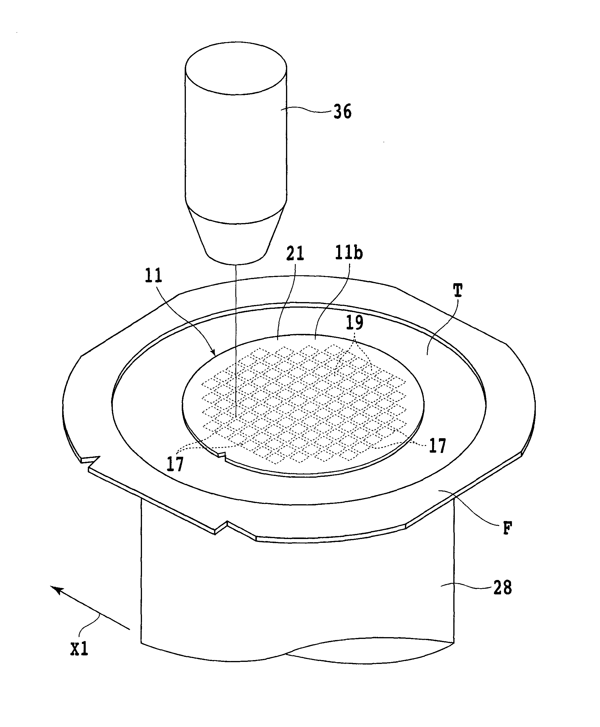
[0033]Now, a splitting method for an optical device wafer according to the present invention is described in detail with reference to FIGS. 5 to 8. In order to carry out the splitting method, preferably the optical device wafer 11 is adhered to a dicing tape T which is an adhesive tape with an outer peripheral portion thereof adhered to an annular frame F, and the optical device wafer 11 is supported by the annular frame F through the dicing tape T as shown in FIG. 5.

[0034]The optical device wafer 11 is sucked to and held by the chuck table 28 of the laser processing apparatus 2 with the dicing tape T interposed therebetween, and the reflective film 21 formed on the reverse surface of the optical device wafer 11 is exposed. Then, an image of the optical device wafer 11 is picked up through the reflective film 21 from the reverse surface 11b side by means of the infrared ray image pickup element of the image pickup means 38 to carry out alignment for aligning a region of the optical ...

second embodiment

[0049]Now, a splitting step is described with reference to FIG. 9. At the splitting step of the present embodiment, a contact preventing film 29 is adhered to the reverse surface 11b of the optical device wafer 11. Then, while the optical device wafer 11 is supported by a pair of support bases 92 of a splitting jig 90 such that the modification layer 23 is positioned at the center between the support bases 92, a wedge member 94 is pressed against the optical device wafer 11 from the front surface 11a side. Consequently, bending stress is generated in a concentrated manner at the portion of the scheduled splitting line 17 having the modification layer 23, and the optical device wafer 11 is split along the scheduled splitting line 17 by the bending stress.

[0050]The splitting jig 90 is successively shifted by a pitch of the scheduled splitting lines 17 so that the optical device wafer 11 is split along all of the scheduled splitting lines 17 extending in the first direction. Then, the...


PUM

PropertyMeasurementUnit
transmittanceaaaaaaaaaa
wavelengthaaaaaaaaaa
transmittanceaaaaaaaaaa

Abstract

In a splitting method for an optical device wafer, the wafer having optical devices formed individually in regions partitioned by a plurality of crossing scheduled splitting lines provided on a front surface and having a reflective film formed on a reverse surface, a focal point of a laser beam is positioned to the inside of the optical device wafer and the laser beam is irradiated along the scheduled splitting lines from the reverse surface side of the wafer to form modification layers in the inside of the wafer. An external force is applied to the wafer to split the wafer along the scheduled splitting lines and form a plurality of optical device chips. The laser beam has a wavelength that produces transmittance through the reflective film equal to or higher than 80%.

Description

BACKGROUND OF THE INVENTION[0001]1. Field of the Invention[0002]This invention relates to a splitting method for an optical device wafer in which a light emitting layer having a plurality of optical devices is formed by epitaxial growth on a substrate for crystal growth of sapphire or the like.[0003]2. Description of the Related Art[0004]By a fabrication process of an optical device such as a laser diode (LD) or a light emitting diode (LED), an optical device wafer is fabricated in which a light emitting layer (epitaxial layer) having a plurality of optical devices is formed by, for example, epitaxial growth on an upper face of a substrate for crystal growth formed from sapphire, SiC or the like. An optical device such as an LD or an LED is formed in each of regions partitioned by scheduled splitting lines formed like a lattice, and individual optical devices are fabricated by splitting the optical device wafer along the scheduled splitting lines into pieces.[0005]Conventionally, as...

Claims


Application Information

Patent Timeline
Patent Type & Authority Applications(United States)
IPC IPC(8): H01L21/78H01L21/301
CPCB23K26/38H01L33/0095B23K26/4075B23K26/0853B23K26/40B23K2103/50H01L21/02H01L21/02266H01L21/302H01L21/304H01L21/30625H01L21/3065H01L21/4896H01L21/76825H01L21/76826H01L21/78
Inventor UENO, HIROUMIHOSHINO, HITOSHI
Owner DISCO CORP
Why Eureka
Try Eureka