Semiconductor device, solid-state image sensor and camera system

a solid-state image sensor and semiconductor technology, applied in the field of semiconductor devices, solid-state image sensors and camera systems, can solve the problems of increasing the number of processes, high cost, and degradation of imaging devices, and achieve the effect of reducing the influence of noise at the connection between chips and cos

Inactive Publication Date: 2012-11-22
SONY CORP
View PDF22 Cites 76 Cited by
  • Summary
  • Abstract
  • Description
  • Claims
  • Application Information

AI Technical Summary

Benefits of technology

[0013]According to the present invention, the influence of noise at the connection between chips can be reduced, a special circuit for communication is not needed and the cost can be reduced as a result.

Problems solved by technology

A process combining a CIS process and a high-speed logic process for integration on one chip, however, results in an increase in the number of processes and high cost, and moreover, it is difficult for such process to produce both analog characteristics and logic characteristics, which may cause degradation in the characteristics of the imaging device.

Method used


Image

  • Semiconductor device, solid-state image sensor and camera system
  • Semiconductor device, solid-state image sensor and camera system
  • Semiconductor device, solid-state image sensor and camera system

Examples


Embodiment Construction

[0036]An embodiment of the present invention will be described below with reference to the drawings.

[0037]The description will be made in the following order:

1. Outline of solid-state image sensor;

2. Process flow;

3. Circuit layout; and

4. TCV (through contact via) layout.

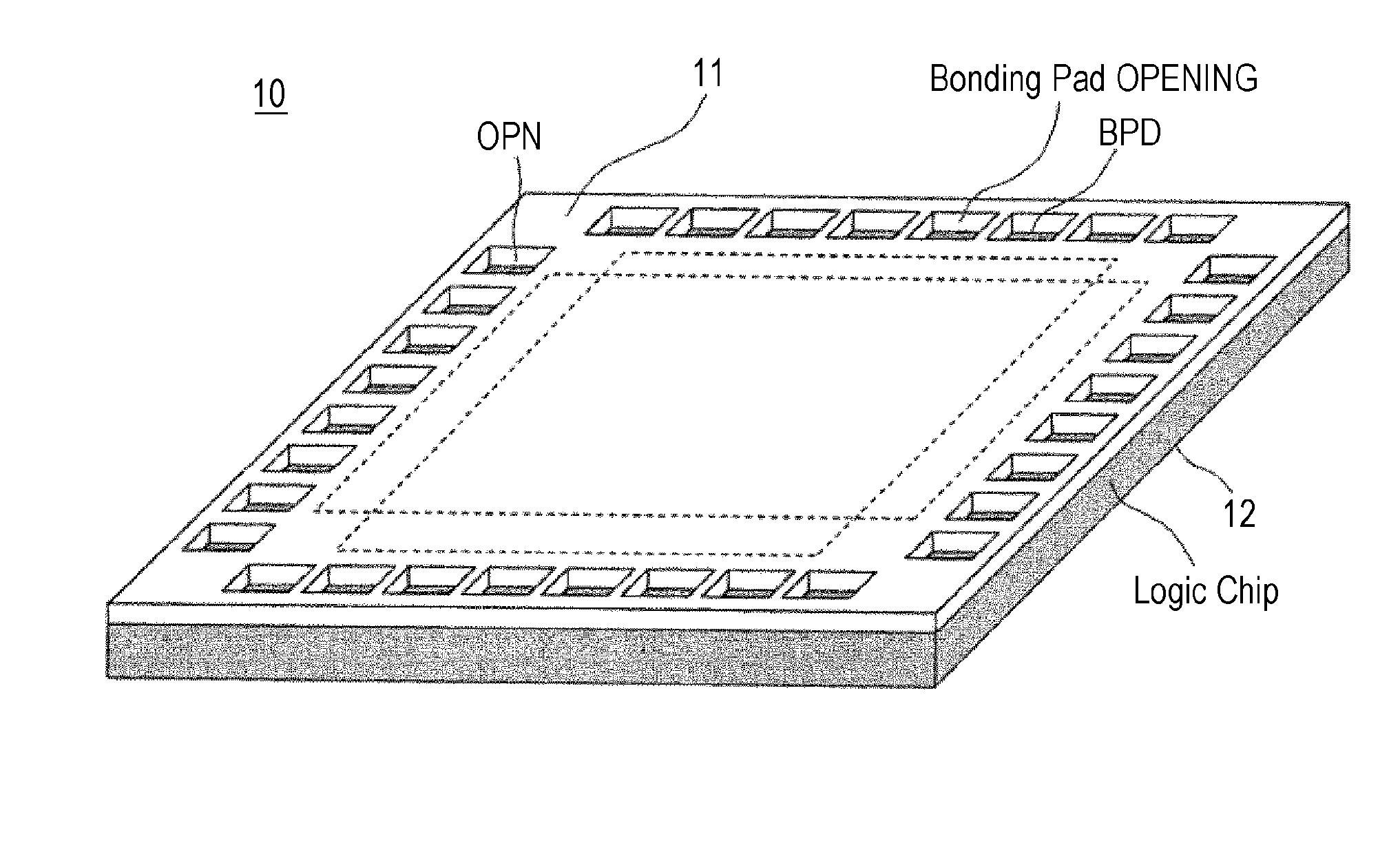
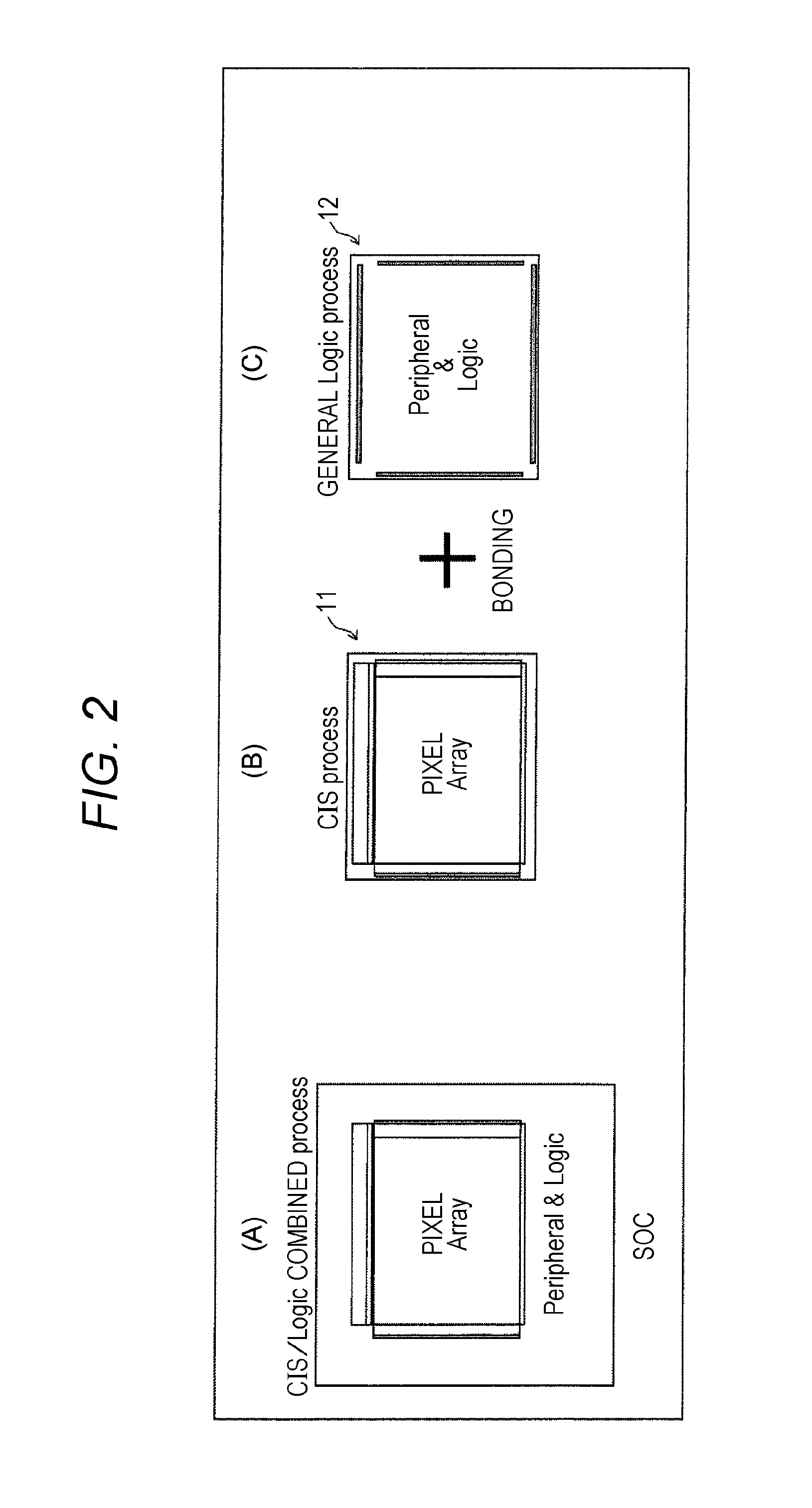
[0038]FIG. 1 is a diagram illustrating an exemplary configuration of a solid-state image sensor that is a semiconductor device according to the embodiment of the present invention.

[0039]In the embodiment, a configuration of a CMOS image sensor will be described as an example of the semiconductor device.

[0040]As illustrated in FIG. 1, a solid-state image sensor 10 has a stacked structure including a first chip (upper chip) 11 and a second chip (lower chip) 12.

[0041]The solid-state image sensor 10 is formed as an imaging device having a stacked structure through bonding at the wafer level and then cutting by dicing as will be described later.

[0042]In the stacked structure including the two upper and lower chips, the fi...


PUM


Abstract

The present invention relates to a semiconductor device, a solid-state image sensor and a camera system capable of reducing the influence of noise at a connection between chips without a special circuit for communication and reducing the cost as a result. The semiconductor device includes: a first chip 11; and a second chip 12, wherein the first chip 11 and the second chip 12 are bonded to have a stacked structure, the first chip 11 has a high-voltage transistor circuit mounted thereon, the second chip 12 has mounted thereon a low-voltage transistor circuit having lower breakdown voltage than the high-voltage transistor circuit, and wiring between the first chip and the second chip is connected through a via formed in the first chip.

Description

TECHNICAL FIELD[0001]The present invention relates to a semiconductor device having a stacked structure of two chips, a solid-state image sensor and a camera system.BACKGROUND ART[0002]In related art, an imaging device is assembled as a module in which two chips, which are a CMOS image sensor (CIS) chip and an image processor chip, are respectively mounted on packages.[0003]Alternatively, the chips may be mounted chip-on-board (COB).[0004]Recently, there has been a need for reduction in mounting areas and in size for mounting an imaging device on a cellular phone or the like, and a System on Chip (SOC) that integrates the two chips on one chip has been developed (see FIG. 2(A)).[0005]A process combining a CIS process and a high-speed logic process for integration on one chip, however, results in an increase in the number of processes and high cost, and moreover, it is difficult for such process to produce both analog characteristics and logic characteristics, which may cause degrada...

Claims


Application Information

Patent Timeline
Patent Type & Authority Applications(United States)
IPC IPC(8): H01L23/498H04N5/335H04N5/225H01L27/146
CPCH01L25/167H01L25/18H01L27/14618H01L27/14621H01L2924/0002H01L27/14627H01L2924/00H01L27/14636H01L27/14634H01L27/14645H01L27/1469H01L27/14698H01L27/14643H04N25/70H04N25/79H04N25/77H04N25/772
Inventor SUKEGAWA, SHUNICHIFUKUSHIMA, NORIYUKI
Owner SONY CORP
Why Eureka
Try Eureka