Supercharge Your Innovation With Domain-Expert AI Agents!

Method for manufacturing a LED array device, and LED array device manufactured thereby

a technology of led array and array device, which is applied in the direction of solid-state devices, light therapy, therapy, etc., can solve the problems of difficult to provide a stimulus of a desired pattern to the brain, light may be irradiated to unwanted parts of the skin, and damage to the brain, so as to facilitate uneven surface stimulation, prevent the effect of light intensity reduction caused by the distance from the light source and easy to understand neural circuitry

Inactive Publication Date: 2012-11-22
KOREA ADVANCED INST OF SCI & TECH
View PDF5 Cites 35 Cited by
  • Summary
  • Abstract
  • Description
  • Claims
  • Application Information

AI Technical Summary

Benefits of technology

"The present disclosure is about a method for making a flexible LED device that can be used for photostimulation, particularly in medical applications. The device is made by separating an LED device from a sacrificial substrate and transferring it to a plastic substrate. This allows for easy stimulation of uneven surfaces of the brain and provides a more efficient and flexible way to provide stimulation without damaging the brain or requiring additional surgery. The flexible LED device can also be used for optogenetics, a technique for controlling neurons using light. The method includes using a laser or LED device to stimulate the skin, but the distance between the light source and the skin can cause a decrease in light intensity. The present disclosure provides a solution by using a flexible LED device that can be easily implanted and can provide high-intensity light to the skin. The flexible LED device is biocompatible and can be attached directly to the skin for effective stimulation. The design features of the patent text include the use of a flexible substrate, the separation of the LED device from a sacrificial substrate, and the transfer of the LED device to a plastic substrate."

Problems solved by technology

However, this method may result in brain damage and it is difficult to provide a stimulus of a desired pattern to the brain since the site of stimulation is restricted to a specific area.
That is to say, the problem of the existing techniques arises because the light source is made of a hard material whereas the brain is round and has many crevices.
However, since these skin therapies involve radiation of light from a long distance using expensive light irradiation devices, the light may be irradiated to unwanted part of the skin and the light intensity decreases due to the long distance from the light source to the skin.

Method used


Image

  • Method for manufacturing a LED array device, and LED array device manufactured thereby
  • Method for manufacturing a LED array device, and LED array device manufactured thereby
  • Method for manufacturing a LED array device, and LED array device manufactured thereby

Examples


Embodiment Construction

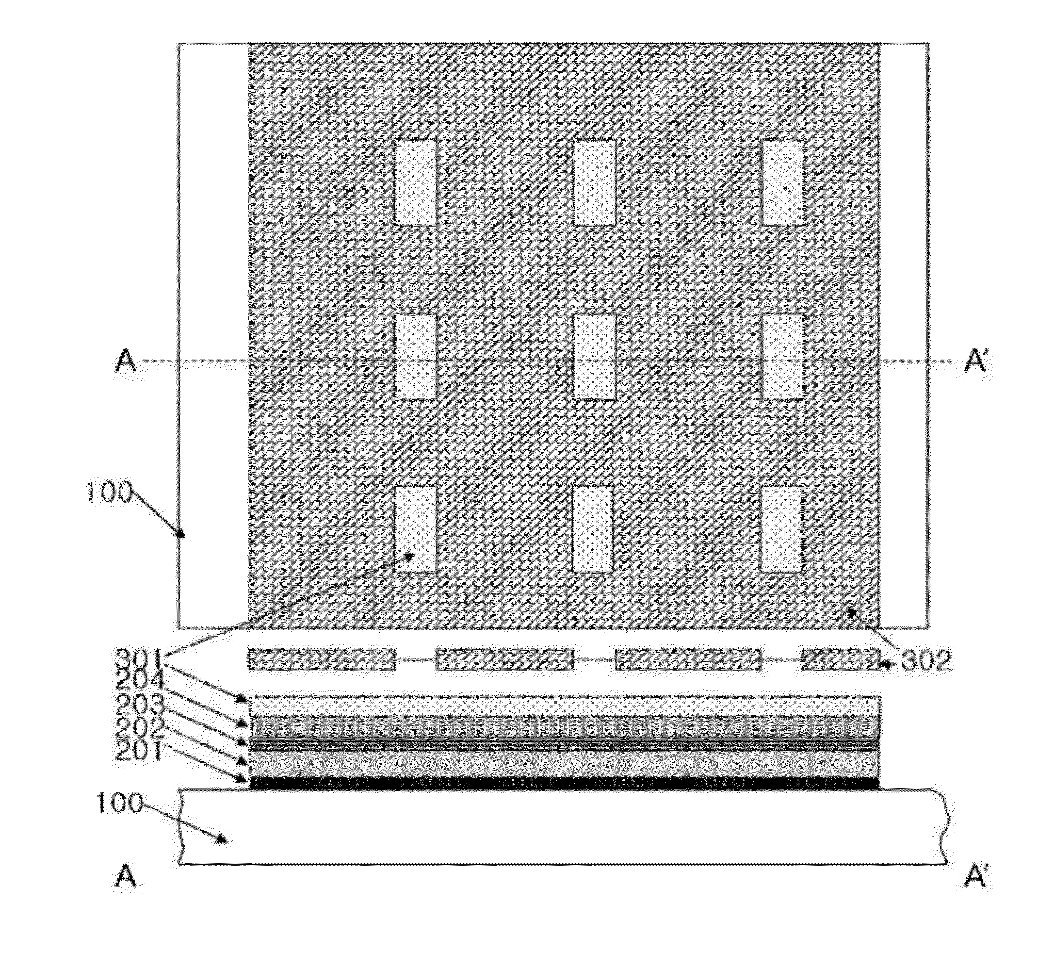
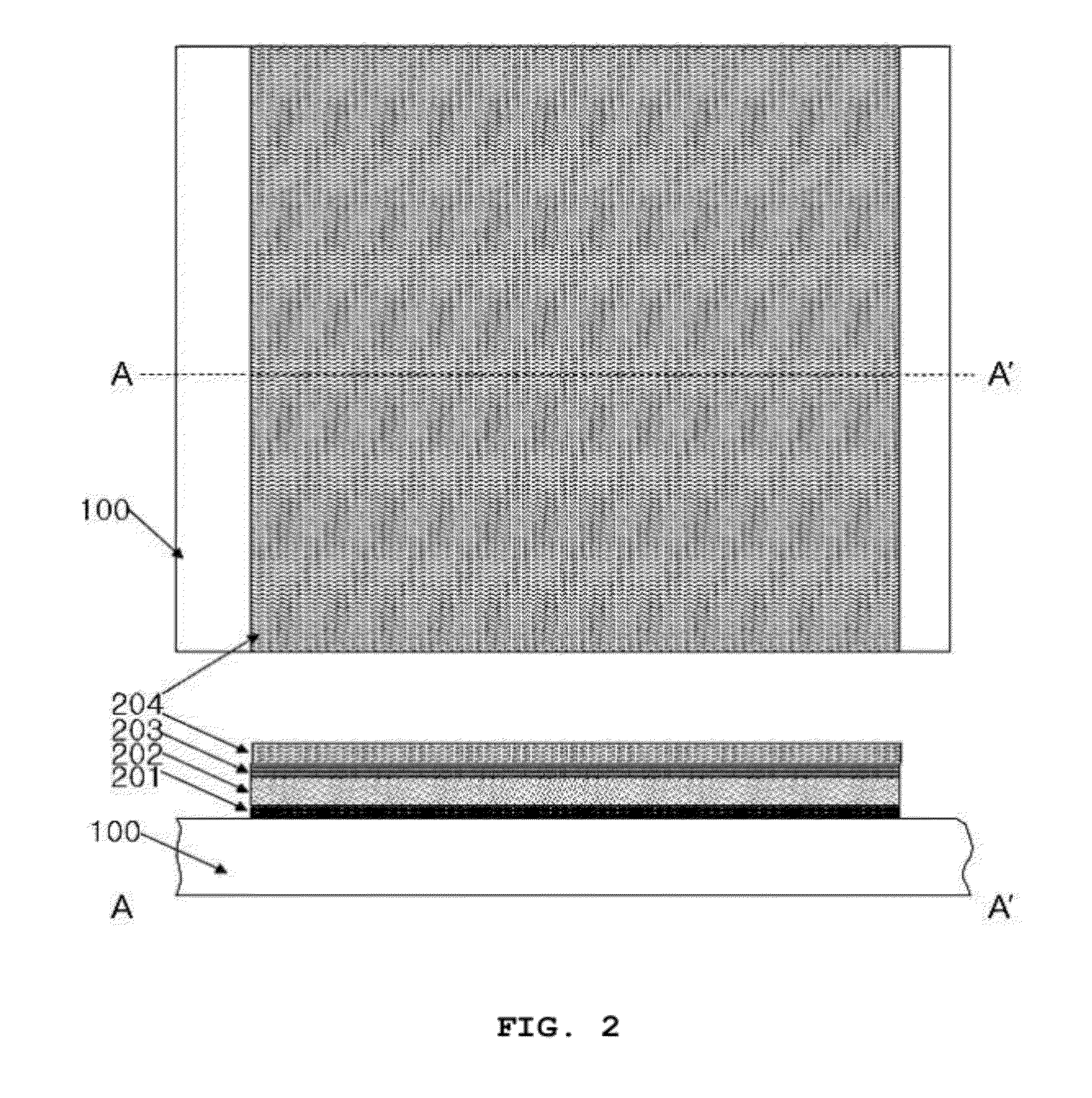
[0014]Hereinafter, the embodiments of the present disclosure will be described in detail with reference to specific examples and accompanying drawings. The following examples are provided for illustrative purposes only and not intended to limit the scope of the present disclosure. Those skilled in the art will appreciate that the present disclosure can be embodied in other forms without being limited to the examples. In the attached drawings, the specific design features of the drawings, including, for example, width, length, thickness, etc. may be somewhat exaggerated for convenience of description. Throughout the specification, the same reference numerals refer to the same elements.

[0015]And, all the attached drawings are plan views or partial cross-sectional views along the line A-A′.

[0016]As used herein, the term “ plastic substrate” is understood to include all substrates having flexible properties. More specifically, it refers to a flexible polymer substrate.

[0017]FIGS. 1-24 s...


PUM


Abstract

Disclosed are a method for fabricating a GaN LED array device for optogenetics and a GaN LED array device fabricated thereby.

Description

TECHNICAL FIELD [0001]The present disclosure relates to a method for fabricating an LED array device and an LED array device fabricated thereby. More particularly, the disclosure relates to a method for fabricating an LED array device which has light weight, is implantable and can be used in a small space through size control via a simple economical process, and an LED array device fabricated thereby.BACKGROUND ART [0002]Light-emitting diode (LED) devices are used for various purposes. One of the applications of the device is a medical application using light of specific frequency. An example is the field of optogenetics, which combines optics with genetics. The concept was developed and advanced by Professor Deisseroth's group at Stanford University. The optogenetics is a cutting-edge technology of controlling neurons. After inserting cell membrane protein genes sensitive to light such as channelrhodopsin-2 (ChR2; responds to blue light emitted from GaN) into the neurons of an expe...

Claims


Application Information

Patent Timeline
Patent Type & Authority Applications(United States)
IPC IPC(8): H01L33/30H01L33/08
CPCA61N5/0622H01L25/0753H01L33/62A61N2005/0652A61N2005/0662H01L2924/12041H01L24/18H01L2924/00H01L24/19H01L2224/24137H01L2224/32225H01L2224/73267H01L2224/92244H01L2924/12042
Inventor LEE, KEON JAEPARK, SO YOUNGLEE, SEUNG HYUNPARK, KWI ILKOO, MIN
Owner KOREA ADVANCED INST OF SCI & TECH
Features
  • R&D
  • Intellectual Property
  • Life Sciences
  • Materials
  • Tech Scout
  • Unparalleled Data Quality
  • Higher Quality Content
  • 60% Fewer Hallucinations
Learn More