
Solar Panel with Energy Efficient Bypass Diode System

a technology of bypass diodes and solar panels, applied in the field of solar panels, can solve the problems of limiting the lifetime of solar panels

Inactive Publication Date: 2012-11-29
RFMARQ
View PDF4 Cites 32 Cited by
  • Summary
  • Abstract
  • Description
  • Claims
  • Application Information

AI Technical Summary

Benefits of technology

[0015]According to one embodiment of the present invention, a solar panel including N panel sections connected in series between an anode terminal and a cathode terminal where N is two or more and each panel section includes one or more solar cells and has an individual bypass diode connected in parallel with and in opposite polarity to the respective panel section includes a panel bypass diode connected between the anode terminal and the cathode terminal of the solar panel where the panel bypass diode is connected in parallel with and in opposite polarity to the solar panel. In operation, the panel bypass diode is fully forward biased by one diode voltage to conduct current through the solar panel when the N panel sections experience performance degradation.

Problems solved by technology

Because a single solar panel can only produce a limited amount of power, most photovoltaic installations involve connecting multiple solar panels into an array.
One of the lifetime-limiting factors for solar panels is hot spots that may be formed on a panel.
Hot spots on a solar panel may limit the panel's lifetime by causing damage to the solar cells or interconnections due to the heat generated by the hot spots.
Hot spots can also cause longer term degradation of the solar cell material.
While some causes of solar panel hot spots are manufacturing related, other causes are beyond the control of the solar panel manufacturer.
When one or more solar cells experiences performance degradation, a reduction in the current generating ability at the degraded solar cells results.
To keep up with the higher current demanded by the load, the degraded solar cells become reverse biased which leads to dissipation of a large amount of power generated by the normal solar cells.
The power dissipation, in the form of heat, leads to “hot spot” formation in the solar panel, with the potential to cause permanent damage to the solar panel.
However, if a solar panel or a portion of a solar panel (e.g. solar panel 2) becomes unable to generate enough current to meet the load current demand, such as because the solar panel is damaged or is shaded from the sun, the affected solar panel (solar panel 2) becomes reverse biased and the associated bypass diode (D2) becomes forward biased and conducts current, thereby allowing excessive current from the normally functioning solar panel 3 to flow in the bypass diode circuit (current path 28) to solar panel 1.
When a single bypass diode is used, the entire solar panel is bypassed even though only one or a few solar cells in the panel may be defective or degraded.
However, when one or more solar cells in a section of the solar panel malfunctions or underperforms, that panel section becomes reverse biased.
However, when the bypass diodes are forward biased and conducts the current from the normally functioning solar panels or solar panel sections, the forward biased bypass diode can dissipate considerable amount of power.
Power dissipation at the bypass diodes results in significant heating of the diode devices and also results in temperature increase in the junction box housing.
In the case of a solar panel with multiple panel sections and multiple bypass diodes, such as solar panel 30 of FIG. 4, significant heating of the bypass diodes can result when multiple panel sections suffer from performance degradation and multiple bypass diodes are forward biased.
The high temperature in the junction box resulted from the power dissipation of the forward biased bypass diodes leads to reliability issues.
Also, power dissipation at the bypass diodes reduces the efficiency of the solar panel.
However, the total power dissipation is not reduced and the efficiency of the solar panel is not improved.

Method used


Image

  • Solar Panel with Energy Efficient Bypass Diode System
  • Solar Panel with Energy Efficient Bypass Diode System
  • Solar Panel with Energy Efficient Bypass Diode System

Examples


Embodiment Construction

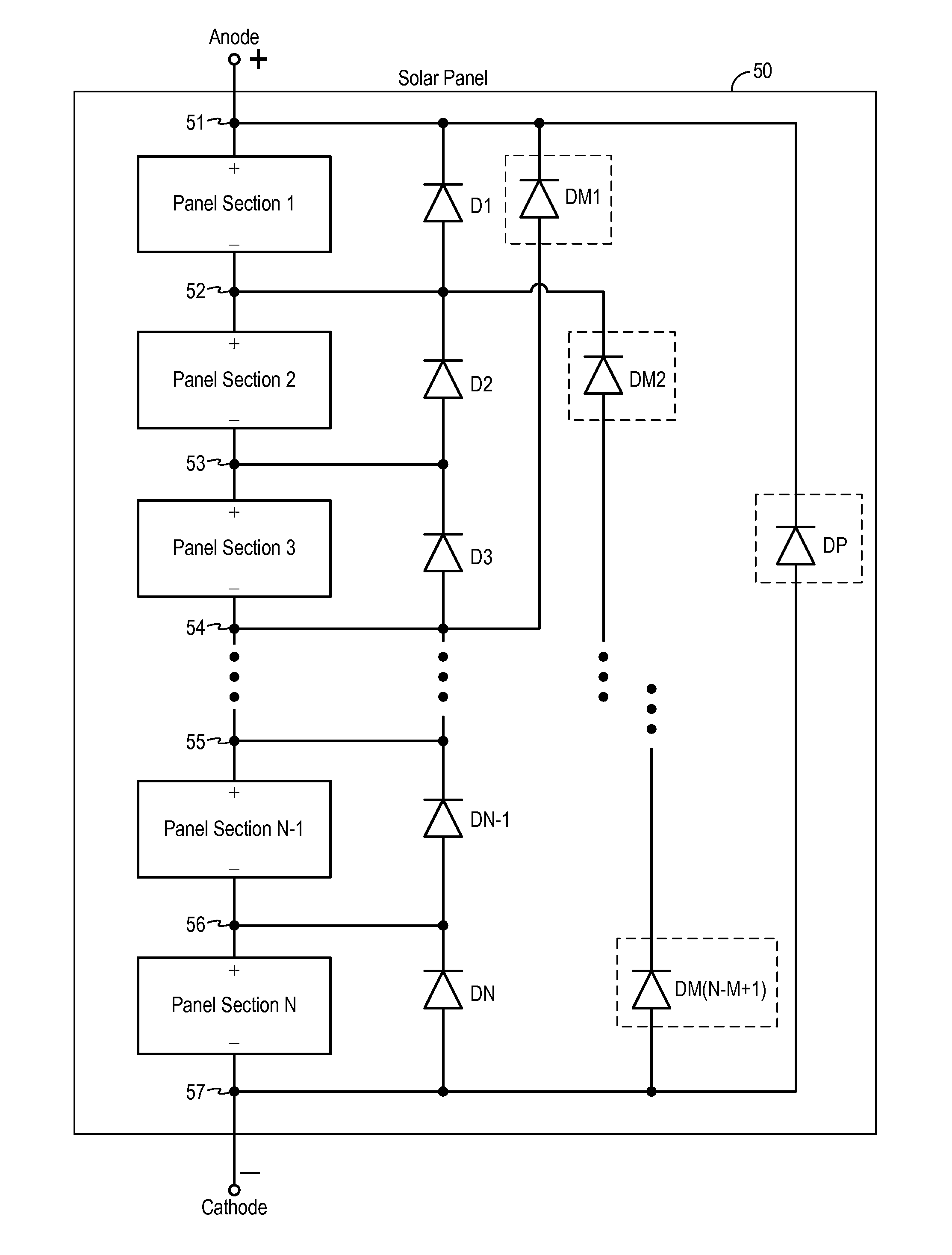
[0030]According to one aspect of the present invention, a system and method to reduce power dissipation at solar panel bypass diodes and improve the energy efficiency of a solar panel with multiple panel sections includes coupling a panel bypass diode across the anode and cathode terminals of the solar panel and coupling one or more group bypass diodes to groups of adjacent panel sections, when the solar panel includes three or more panel sections. In this manner, when two or more adjacent panel sections in a solar panel experience performance degradation, the panel bypass diode or the group bypass diode is forwarded biased to provide a current path to bypass the degraded panel sections, instead of allowing the current to flow through the individual bypass diode coupled to each individual panel section. As a result, a fewer number of bypass diodes is forward biased and conducting currents when multiple adjacent panel sections experience performance degradation so that the power diss...


PUM


Abstract

A solar panel including N panel sections and individual bypass diodes for each panel section includes a panel bypass diode connected in parallel with and in opposite polarity to the solar panel. The solar panel may further include one or more group bypass diodes when the solar panel includes three or more panel sections. Each group bypass diode is connected across a group of M adjacent panel sections, M being selected from 2 to N−1. The group bypass diode is connected in parallel with and in opposite polarity to the group of M adjacent panel sections. A group bypass diode is fully forward biased to conduct current through the solar panel when the associated group of M adjacent panel sections experience performance degradation. The panel bypass diode is fully forward biased to conduct current through the solar panel when the N panel sections experience performance degradation.

Description

FIELD OF THE INVENTION[0001]The invention relates to solar panels and, in particular, to a system and a method for improving energy efficiency of bypass diodes installed in solar panels.DESCRIPTION OF THE RELATED ART[0002]A solar panel, also referred to as a photovoltaic panel, a solar module, or a photovoltaic module, is a packaged interconnected assembly of solar cells (also referred to as “solar wafers” or “photovoltaic cells”). FIG. 1(a) illustrates a conventional solar panel 1 including an assembly of solar cells 2 interconnected in a two-dimensional array. Solar panels use light energy (photons) from the sun to generate electricity through photovoltaic effect (i.e., the photo-electric effect). In a solar panel, the solar cells are connected electrically in series and in parallel to generate the desired output voltage and output current. More specifically, solar cells in a solar panel are connected in series to create an additive voltage and connected in parallel to yield a hig...

Claims


Application Information

Patent Timeline
Patent Type & Authority Applications(United States)
IPC IPC(8): H01L31/05G05F1/10
CPCH01L31/044Y02E10/50
Inventor CHEN, HSI SHENGCHEN, YU-CHIH
Owner RFMARQ
Features
  • Generate Ideas
  • Intellectual Property
  • Life Sciences
  • Materials
  • Tech Scout
  • Unparalleled Data Quality
  • Higher Quality Content
  • 60% Fewer Hallucinations
Learn More