
Amplifier Component Comprising A Compensation Element

a compensation element and amplifier technology, applied in the direction of amplifiers, amplifiers with semiconductor devices/discharge tubes, semiconductor devices, etc., can solve the problems of reducing the bandwidth of the matching network, requiring a relatively large and expensive chip housing form, and additional insulating layers, so as to reduce couplings and avoid further undesirable resonances

Active Publication Date: 2012-11-29
ROHDE & SCHWARZ GMBH & CO KG
View PDF4 Cites 2 Cited by
  • Summary
  • Abstract
  • Description
  • Claims
  • Application Information

AI Technical Summary

Benefits of technology

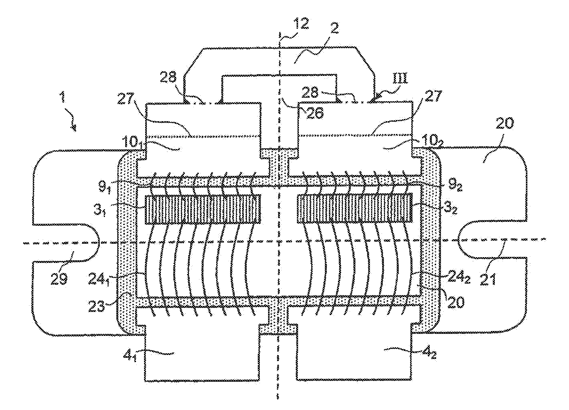
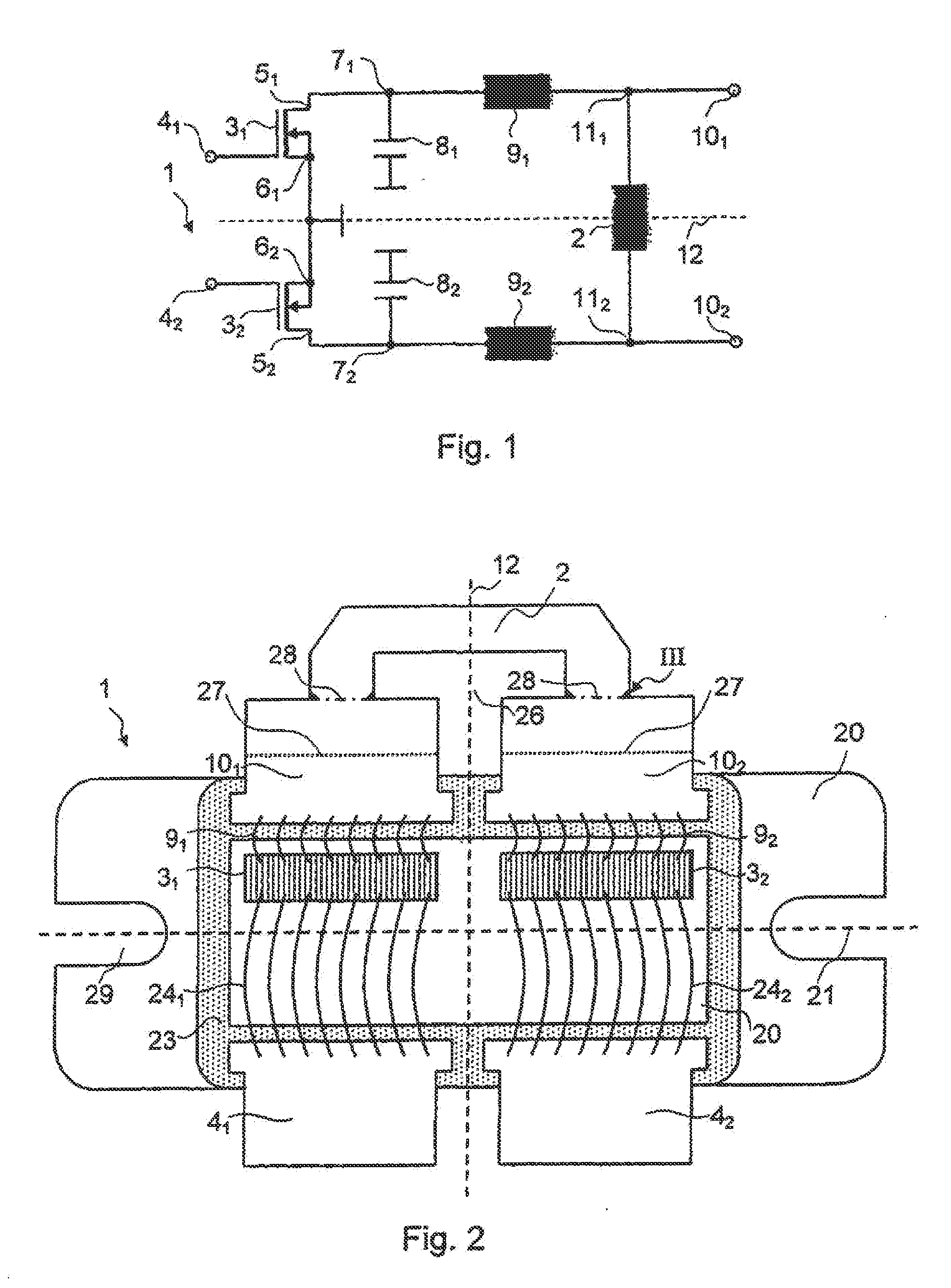
[0011]A further advantage of the invention is that the connecting pins of the chip housing and the compensation element formed as a connecting lug are embodied in one part. This means that the compensation element can be added directly in the manufacturing process for the chip housing and no additional soldering process is necessary. Accordingly, it can be guaranteed that the inductance of each individual compensation element is always of an identical magnitude.
[0012]A further advantage of the invention is achieved if the connecting pins of the chip housing provide a bending edge. Accordingly, the compensation element can be bent in such a manner that an angle of preferably 45′ to 135′, by particular preference of 90° is formed between the compensation element and the connecting pins of the chip housing. This achieves a further reduction of the couplings.
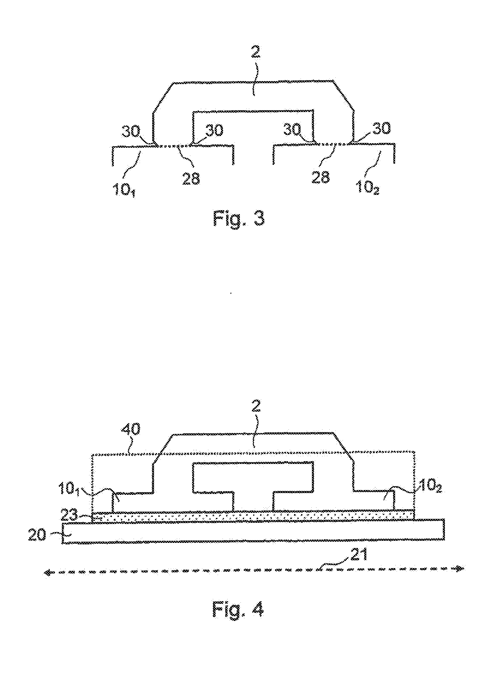
[0013]Furthermore, it is advantageous that the compensation element formed as a connecting lug can be separated from the connecting pins of the chip housing at a break-off point or a narrowing. As a result, the same amplifier component can also be used for applications in which such a compensation element would be associated with disadvantages.
[0014]Moreover, it is advantageous that the compensation element formed as a connecting lug can be embodied in different ways in order to compensate parasitic output capacitances of different magnitude in a simple manner without having to vary the chip design in every case.
[0015]A further advantage of the invention is that the two amplifier elements are power transistors, preferably LDMOS transistors (laterally diffused metal-oxide semiconductor; lateral diffused metal-oxide semiconductor), which are arranged in a so-called push-pull configuration. In this context, a supply voltage of identical magnitude is supplied to the drain connections of both power transistors, so that the compensation element can be arranged in series between the two drain connections without an additional capacitor for direct-voltage de-coupling, thereby avoiding further undesirable resonances.
[0016]Various exemplary embodiments of the invention are described by way of example below with reference to the drawings. Identical subject matters provide the same reference numbers.

Problems solved by technology

The disadvantage with U.S. Pat. No. 4,107,728 is that a relatively large and expensive chip housing forms are necessary for the realization of such an integrated shunt inductance.
The mutual inductance resulting from the coupling has a disadvantageous effect on the compensation behavior, so that, ultimately, the bandwidth of the matching network is reduced.
Moreover, such a shunt inductance which is realized as a printed conductor cannot be applied directly to the flange, but requires an additional insulating layer.

Method used


Image

  • Amplifier Component Comprising A Compensation Element
  • Amplifier Component Comprising A Compensation Element
  • Amplifier Component Comprising A Compensation Element

Examples


Embodiment Construction

[0026]The following discussion provides many example embodiments of the inventive subject matter. Although each embodiment represents a single combination of inventive elements, the inventive subject matter is considered to include all possible combinations of the disclosed elements. Thus if one embodiment comprises elements A, B, and C, and a second embodiment comprises elements B and D, then the inventive subject matter is also considered to include other remaining combinations of A, B, C, or D, even if not explicitly disclosed.

[0027]FIG. 1 shows a circuit diagram (equivalent circuit diagram) of the amplifier component 1 with the compensation element 2 according to the invention. The amplifier component 1 is structured in mirror-image symmetry about the axis 12. The amplifier component 1 provides at least two amplifier elements 31, 32, which are controlled preferably in phase opposition and arranged in a push-pull configuration. The amplifier elements 31, 32 can also be referred t...


PUM


Abstract

An amplifier component (1) provides a chip housing (40) and at least two amplifier elements (31, 32). Between at least two connections (51, 52 and 61, 62) of each amplifier element (31, 32), a parasitic capacitance (81, 82) is formed, wherein this parasitic capacitance (81, 82) is compensated by an inductive compensation element (2). The compensation element (2) itself is formed between two connecting contacts (101, 102) outside of the chip housing (40) by a connecting lug (2).

Description

[0001]This application is a national phase of International Application PCT / E2010 / 007261, which claims the priority of German Patent Application DE 10 2009 060 669.6, filed Dec. 28, 2009, and German Patent Application DE 10 2010 009 984.8, filed Mar. 3, 2010. International Application PCT / E2010 / 007261, German Patent Application DE 10 2009 060 669.6, and German Patent Application DE 10 2010 009 984.8 are incorporated herein by reference in their entirety.FIELD OF THE INVENTION[0002]The field of the invention is amplifier technologies.BACKGROUND[0003]An amplifier component, especially a high-frequency amplifier component, within a chip housing with a compensation element, can be used in communications technology, for example, for the transmission of radio and television signals, in mobile-radio base stations, in computer measurement technology and for scientific purposes in order to generate large high-frequency powers.[0004]The amplifier component is composed substantially of power t...

Claims


Application Information

Patent Timeline
Patent Type & Authority Applications(United States)
IPC IPC(8): H03F3/26
CPCH01L23/645H01L23/66H01L2223/6655H03F3/193H03F3/265H01L24/48H01L2924/30107H01L2224/48091H01L2224/49175H01L2924/3011H01L24/49H01L2924/1305H01L2924/1306H01L2924/00014H01L2924/00H01L2924/30111H01L2224/45099H01L2224/45015H01L2924/207
Inventor KAEHS, BERNHARD
Owner ROHDE & SCHWARZ GMBH & CO KG
Learn More