Observation method and observation device

a technology of observation device and observation method, which is applied in the direction of closed-circuit television system, television system, electric discharge tube, etc., can solve the problems of inability to obtain sufficient focal point measurement, inability to obtain image contrast, and inability to obtain edge sharpness, etc., to achieve the effect of reducing the influen

Active Publication Date: 2012-11-29
HITACHI HIGH-TECH CORP
View PDF2 Cites 20 Cited by
  • Summary
  • Abstract
  • Description
  • Claims
  • Application Information

AI Technical Summary

Benefits of technology

[0020]With the present invention, it is possible to mitigate the influence that the t...

Problems solved by technology

However, depending on the defect being imaged, or the material or structure of the pattern, there may be cases where image contrast cannot be obtained, edge sharpness decreases, and a sufficient focal point measure cann...

Method used


Image

  • Observation method and observation device
  • Observation method and observation device
  • Observation method and observation device

Examples


example 1

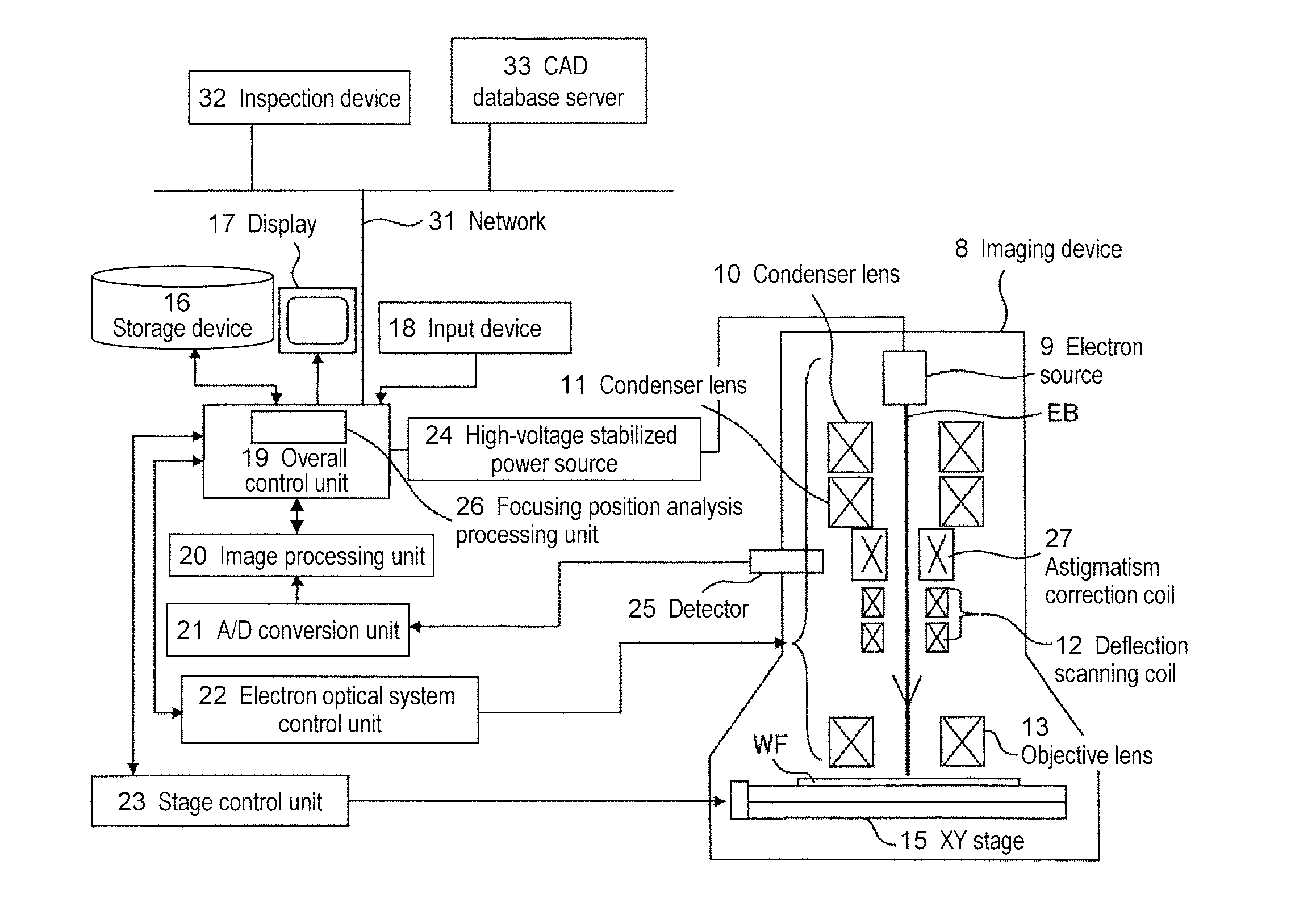
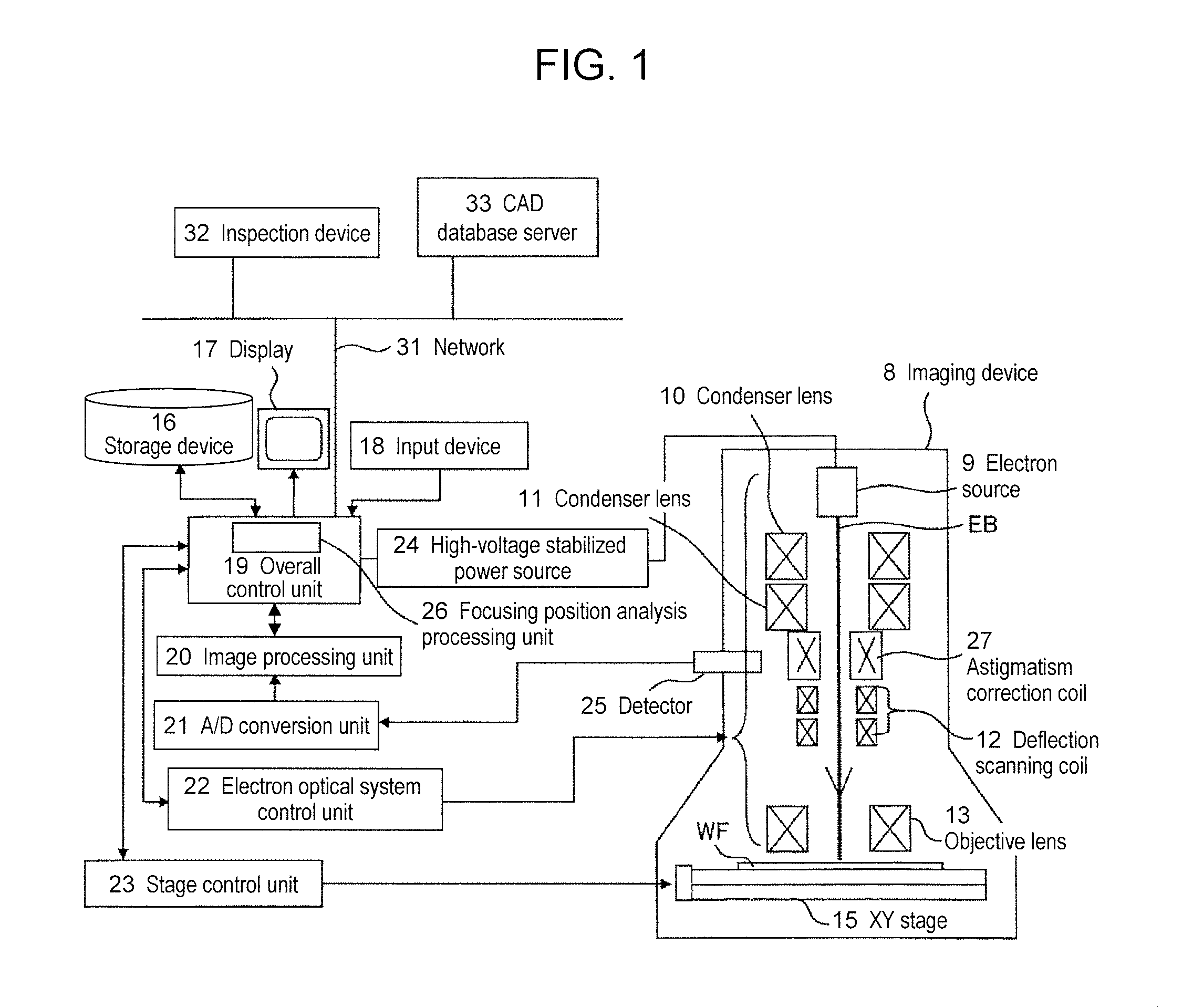
[0032]An embodiment of the present example is described below with reference to the drawings. FIG. 1 is a vertical sectional view showing a general configuration of an electron microscope. With respect to an imaging device 8 of a review SEM device, which is obtained by improving a scanning electron microscope so that it may be used for observing defects in circuit patterns formed on semiconductor wafers, the part between a semiconductor wafer WF and where an electron beam EB is generated is maintained under a vacuum. The imaging device 8 is provided with an electron source 9, condenser lenses 10 and 11, deflection scanning coils 12, an objective lens 13, an astigmatism correction coil 27, an XY stage 15, and a detector 25. In addition, outside of the vacuum device, there are provided a storage device 16, a display 17, an input device 18, an image processing unit 20, an A / D conversion unit 21, an electron optical system control unit 22, a stage control unit 23, and a high-voltage sta...

example 2

[0078]In the present embodiment, a description will be provided with respect to a charged particle device, particularly a defect review device, including a function of determining a step size for autofocusing that employs CAD data that is layout information for a pattern on a semiconductor wafer. Since the hardware configuration of the device is generally the same as that in FIG. 1, descriptions for like parts will be omitted, referring to elements in FIG. 1 where necessary.

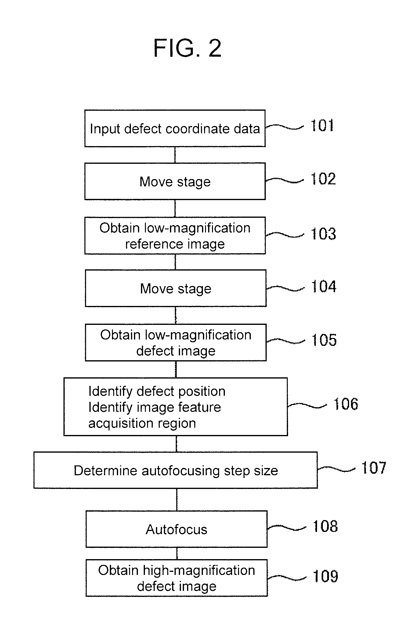
[0079]First, using the flowchart in FIG. 8, a device operation is described where a high-magnification image of a defect present on a sample under observation is obtained. As the operator of the device instructs the reading of defect coordinate data and CAD data through the input device 18, defect coordinate data and CAD data are respectively inputted to the review SEM from the inspection device 32 and the CAD database server 33 via the network 31 (step 701). The term defect coordinate data as used above refers t...


PUM


Abstract

With respect to a charged particle beam device, the step size of focal point measure for executing autofocusing is optimized to a value that is optimal with respect to the spread of an approximation curve for a focal point measure distribution. The step size of focal point measure for executing autofocusing is corrected using an image feature obtained based on a layout image derived from an image obtained at a first magnification or from design data. Autofocusing is executed based on the obtained step size to carry out observation, measurement, or to image the sample under inspection.

Description

TECHNICAL FIELD[0001]The present invention relates to a method of observing a sample using a scanning electron microscope for reviewing defects that have occurred in the process of fabricating semiconductor devices, as well as to a device thereof.BACKGROUND ART[0002]In semiconductor device fabrication processes, in order to observe defects that cause device failures, automatic defect observation is performed wherein an image where a defect detected by an optical inspection device or electron beam-based inspection device is located is re-detected at a high resolution by means of a review SEM device as an application of a scanning electron microscope. Because of the reduction in size of semiconductor device circuit patterns and of the resultant reduction in defect size, such review SEM devices are required to be capable of highly reliable and high-resolution automatic defect observation for defects detected by an inspection device.[0003]With respect to automatic defect observation by ...

Claims


Application Information

Patent Timeline
IPC IPC(8): H04N5/232H04N7/18
CPCH01J37/21H01J37/28H01J2237/221H01J2237/2817H01J2237/216
Inventor BAN, NAOMAOBARA, KENJI
Owner HITACHI HIGH-TECH CORP
Why Eureka
Try Eureka