Supercharge Your Innovation With Domain-Expert AI Agents!

Optical Waveguide Element Module

a technology of optical waveguide elements and modules, applied in non-linear optics, instruments, optics, etc., can solve the problems of difficult to effectively apply modulation signals to optical waveguide elements, difficult to flatten frequency characteristics, and jitter becomes an important issue, so as to achieve parallel circuits easily, the effect of flattening frequency characteristics

Active Publication Date: 2012-11-29
SUMITOMO OSAKA CEMENT CO LTD
View PDF3 Cites 4 Cited by
  • Summary
  • Abstract
  • Description
  • Claims
  • Application Information

AI Technical Summary

Benefits of technology

The invention provides an optical waveguide element module that can suppress reflection of the modulation signal and attenuation of the modulation signal even when the impedance of the modulation electrode is different from the impedance of the transmission line. The module includes a relay line that connects the modulation electrode and the external signal line, which has a stepwise or continuous impedance change to suppress reflection of the modulation signal. The module also includes a filter circuit with a capacitor to adjust the modulation signal. The length of the relay line and the gap between the signal electrode and the ground electrode can be adjusted to achieve a flat optical response frequency characteristic over a wide range of frequencies. The invention provides an improved optical waveguide element module that can suppress reflection and attenuation of the modulation signal and achieve a flat optical response frequency characteristic.

Problems solved by technology

Although such a method of adjusting the impedance provides a certain effect for reflection suppression of the microwave which is a modulation signal, there is a problem in that the microwave is attenuated by the resistor 11, and it is difficult to effectively apply the modulation signal to the optical waveguide element.
In particular, the occurrence of such jitter becomes an important issue in the optical waveguide element having a transmission speed of a gigahertz order.
However, it is difficult to flatten the frequency characteristic up to the high frequency range that allows for several tens of Gbps transmission only using the termination circuit.
While a circuit configuration using such a thin film contributes to the miniaturization of the filter circuit, the manufacturing process becomes complicated, and in particular, a number of processes for forming and removing thin film are necessary to configure the capacitor using the thin film.
However, it is difficult to adjust the value of the capacitor since the trimming may lead to a short circuit between the electrodes.
For this reason, it was considered that the laminated ceramic capacitor is unsuitable for a component of the filter circuit for connecting the optical waveguide element.

Method used


Image

  • Optical Waveguide Element Module
  • Optical Waveguide Element Module
  • Optical Waveguide Element Module

Examples


Embodiment Construction

[0078]Hereinafter, the preferable embodiments of the invention will be described in detail.

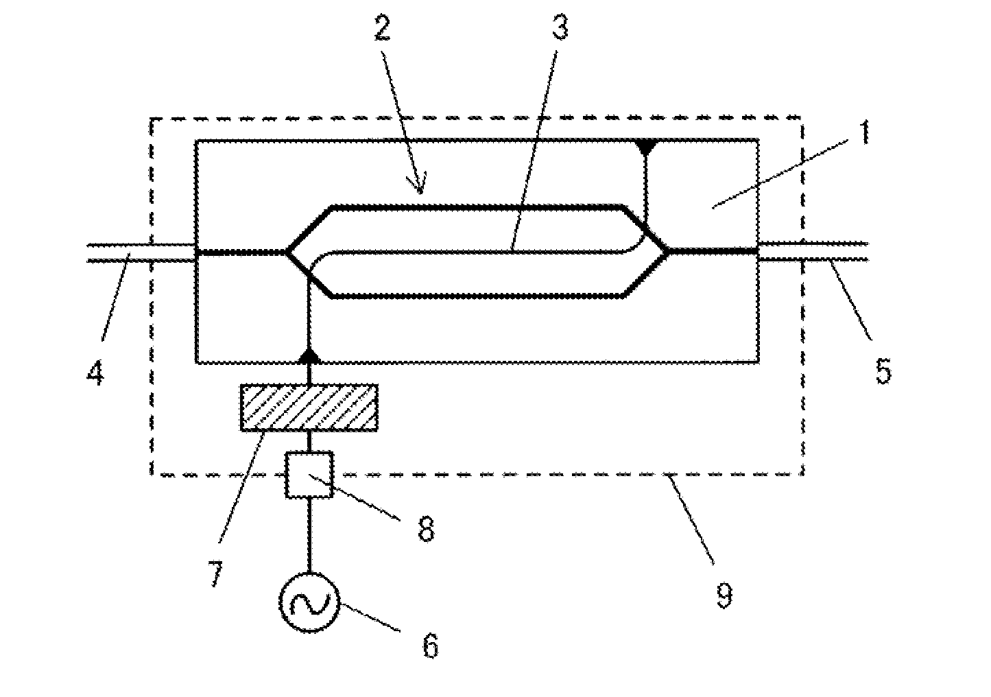
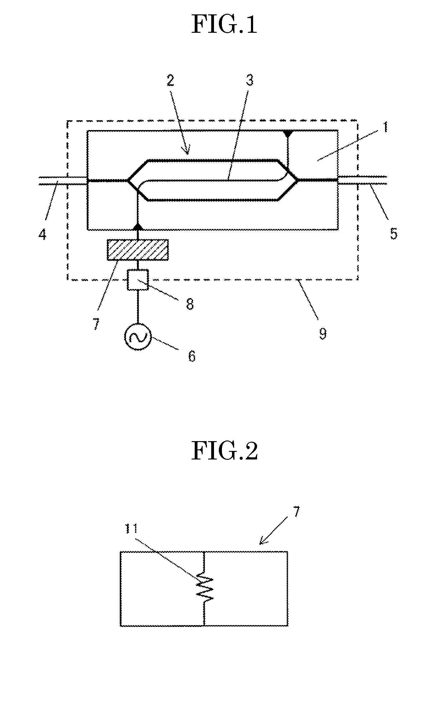
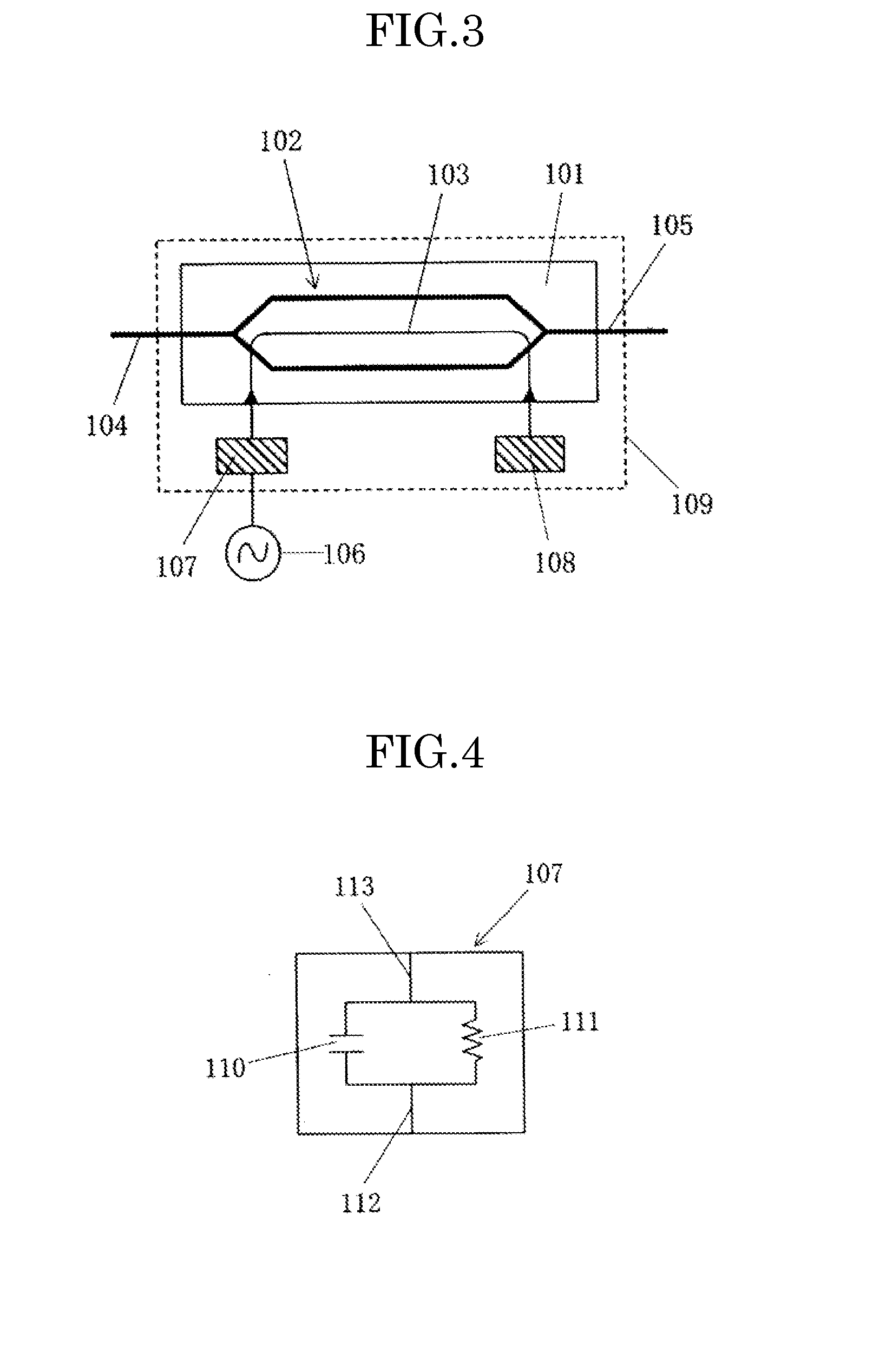
[0079]According to the invention, there is provided an optical waveguide element module including: an optical waveguide formed on a substrate; an optical waveguide element including an optical waveguide element having a modulation electrode for modulating an optical wave propagating through the optical waveguide; a connector where an external signal line for inputting a modulation signal into the modulation electrode is connected; and a relay line formed on the relay substrate to connect the connector and the modulation electrode, wherein the relay line is a coplanar-type line in which a signal electrode is interposed between ground electrodes, an impedance of the relay line changes stepwise or continuously so as to suppress reflection of the modulation signal in the optical waveguide element module, and a filter circuit including a capacitor is arranged in the middle of the relay line.

[0080]I...


PUM

PropertyMeasurementUnit
electrostatic capacitanceaaaaaaaaaa
resonance frequencyaaaaaaaaaa
distanceaaaaaaaaaa

Abstract

An optical waveguide element module includes an optical waveguide formed on a substrate, an optical waveguide element having a modulation electrode for modulating an optical wave propagating through the optical waveguide, a connector where an external signal line for inputting a modulation signal into the modulation electrode is connected, and a relay line formed on a relay substrate to connect the connector and the modulation electrode. The relay line is a coplanar-type line, in which a signal electrode is interposed between ground electrodes. The impedance of the relay line changes stepwise or continuously so as to suppress reflection of the modulation signal in the optical waveguide element module. A filter circuit including a capacitor is arranged in the middle of the relay line.

Description

BACKGROUND OF THE INVENTION[0001]1. Field of the Invention[0002]The present invention relates to an optical waveguide element module, and more particularly, to an optical waveguide element module including a connector where an external signal line for inputting a modulation signal into a modulation electrode of the optical waveguide element is connected, a relay substrate for connecting modulation electrodes of the optical waveguide element and the connector, and the relay substrate having a relay line and a filter circuit on the relay substrate.[0003]2. Description of Related Art[0004]In the fields of optical communication or optical measurement of the related art, an optical waveguide element, where an optical waveguide is formed on a substrate, such as an optical modulator, is widely used as means for controlling the optical wave.[0005]Such an optical waveguide element is provided with a modulation electrode for modulating the optical wave propagating through the optical waveguid...

Claims


Application Information

Patent Timeline
Patent Type & Authority Applications(United States)
IPC IPC(8): G02F1/035
CPCG02F1/0121G02F1/0327G02F1/2255
Inventor SHIMIZU, RYO
Owner SUMITOMO OSAKA CEMENT CO LTD
Features
  • R&D
  • Intellectual Property
  • Life Sciences
  • Materials
  • Tech Scout
  • Unparalleled Data Quality
  • Higher Quality Content
  • 60% Fewer Hallucinations
Learn More