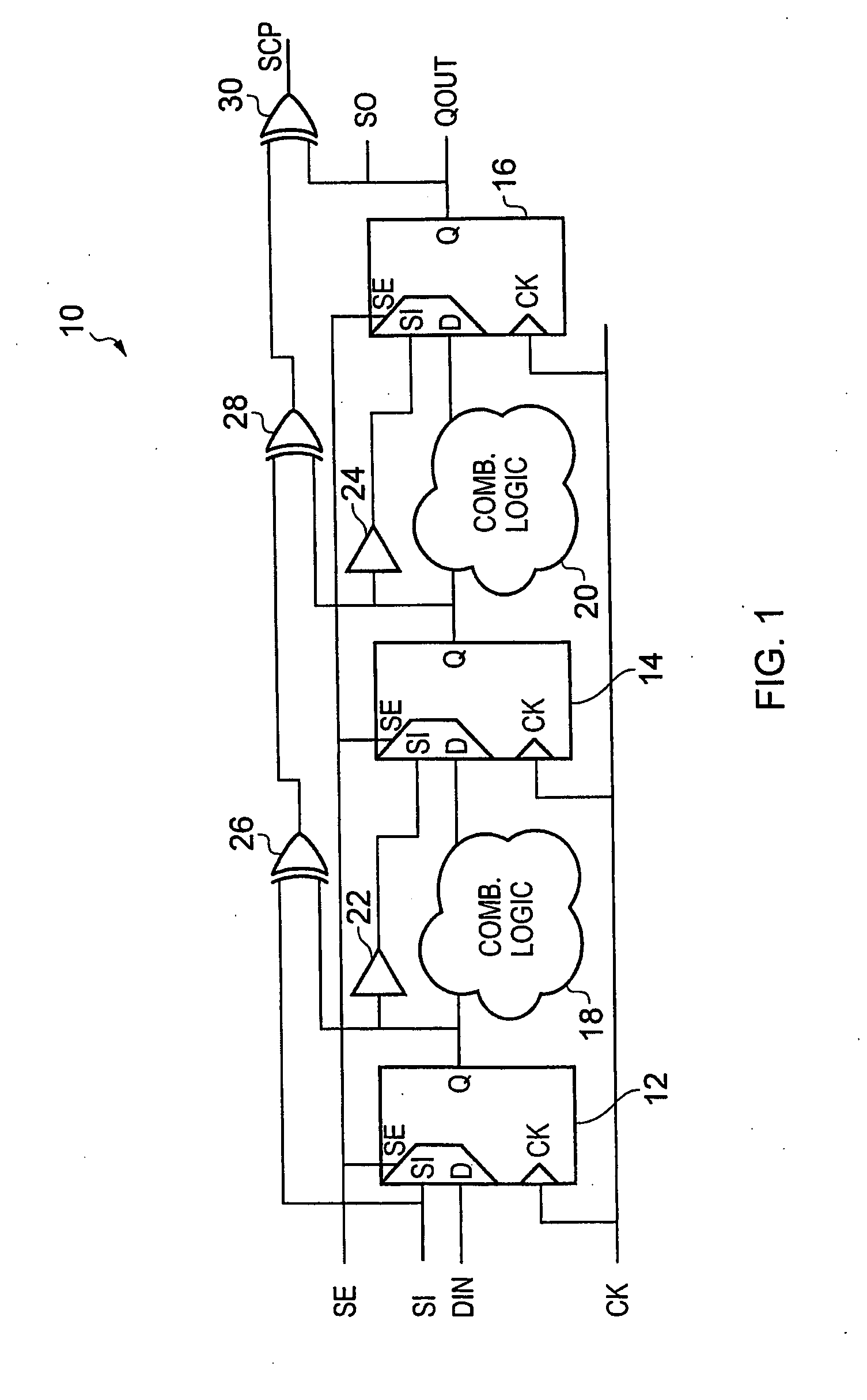
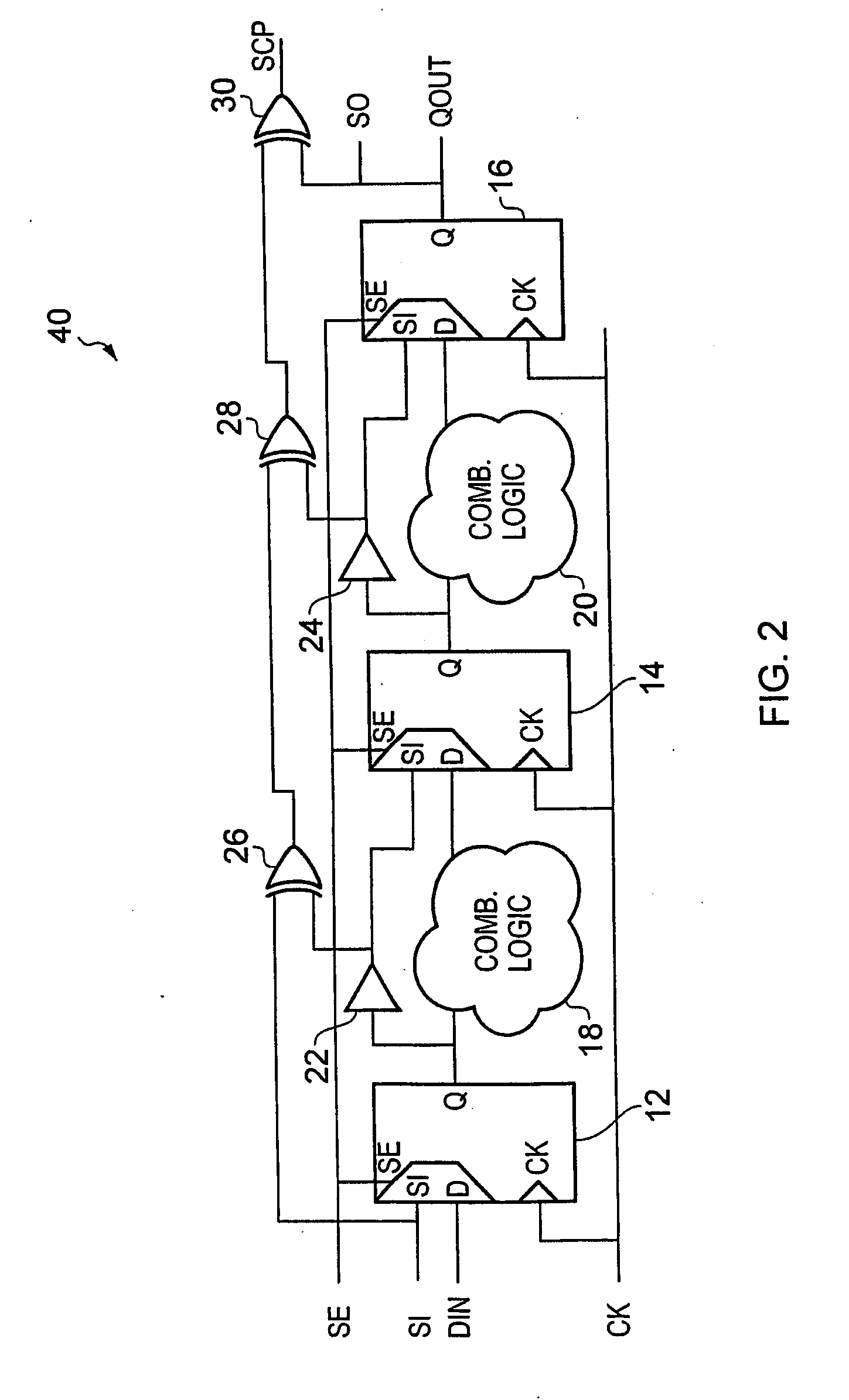
[0026]There are a number of ways in which the parity information generation elements can be arranged to provide the parity path. In one embodiment said parity information generation elements are arranged to provide said parity path by an output of a first parity information generation element forming one input of a next parity information generation element. This
concatenation of the parity information generation elements provides a simple, modular approach to forming the parity path and provides a simple approach for the EDA tools to stitch these parity information generation elements together.
[0028]As mentioned above, the state retention circuits may have separate scan and data outputs (the same being true on the input side), and in one embodiment said plurality of state retention circuits each comprises a scan-in input and a dedicated scan-out output, said dedicated scan-out output of a first state retention circuit being connected to said scan-in input of a next state retention circuit to provide said scan path, wherein said scan path provides said parity path. Accordingly, the existing scan path which connects the state retention circuits together is reused to provide the parity path. In the space-constrained environment of contemporary integrated circuits, this dual use of the scan path is particularly advantageous.
[0029]For such state retention circuits, the parity information generation elements may be provided as separate elements, or may be provided within said plurality of state retention circuits. Providing the parity information generation elements within the state retention circuits can be advantageous, for example in terms of the EDA synthesis, since the EDA tools which are already in use for scan-ready synthesis may be directly reused, simply substituting the state retention circuits of the present technique.
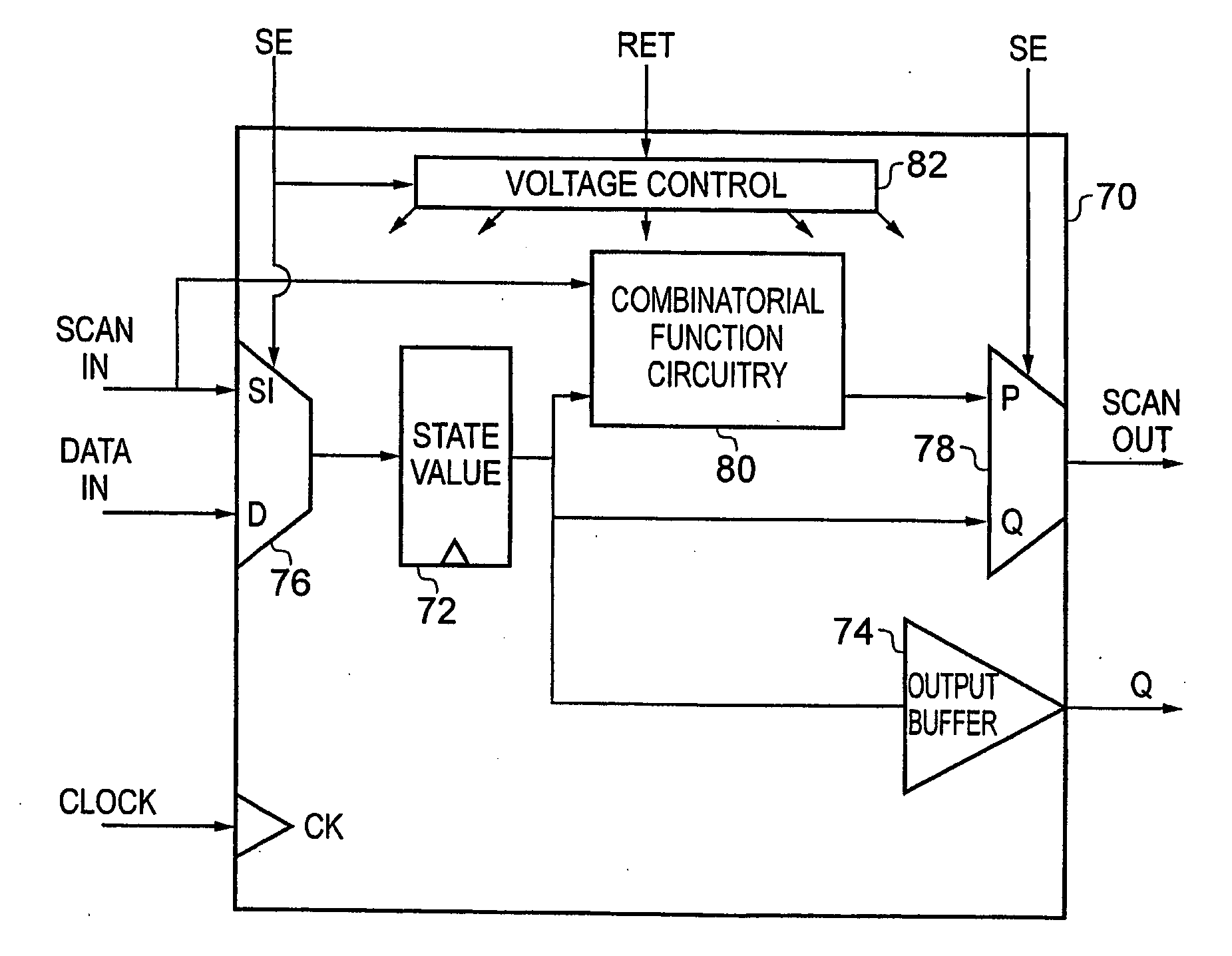
[0033]In one embodiment said plurality of state retention circuits is provided with a retention
voltage supply, said retention
voltage supply being configured to provide a sufficient
voltage to said plurality of state retention circuits to hold said respective state values at said respective nodes of said data processing circuitry when said data processing circuitry enters said low power mode, wherein said plurality of parity information generation elements are powered by said retention voltage supply. Accordingly, by powering the parity information generation elements from the same voltage supply which enables the respective state values to be held during the low power mode, the generation of the parity information is supported when the data processing circuitry enters the low power mode. It is to be noted that for
power saving reasons, the voltage supply provided to the plurality of parity information generation elements can itself be reduced to a “drowsy retention” mode wherein the operation of the parity information generation elements is also at near-threshold. Although this may result in longer propagation times, the parity output may nonetheless be generated and therefore the integrity of the held state values can be monitored.
[0037]In one such embodiment, the apparatus comprises a first set of parity paths and a second set of parity paths, wherein a parity path of said first set of parity paths provides a first output parity value which is dependent on a first set of state values, and wherein output values of more than one parity path of said second set of parity paths are dependent on said first set of state values. One example implementation of this is where the first set of parity paths are essentially orthogonal to the second set of parity paths (e.g. the first set run horizontally whilst the second set run vertically), although there is no need for the two sets to adhere to any particular geometric orientation with respect to one another, nor to follow any particular direction through the apparatus. Nevertheless, it may be beneficial from a
system diagnostic point of view to arrange the first set to provide parity information with respect to a given “direction” through the apparatus, whilst the second set provide parity information with respect to a second “direction” through the apparatus, such that when combined the first and second sets of output parity values can provide complementary information to one another. Given that an individual parity path can only indicate that a state value has changed somewhere along its length, arranging a second set of parity paths which cross that parity path can help to identify where the state value changed. Indeed, where the state retention circuits are coupled to two sets of parity paths which are fully complementary to one another, the two sets of output parity values can effectively provide a coordinate
system by which the state retention circuit responsible for the state value which has changed can be identified. Accordingly, in one embodiment said first set of parity paths and said second set of parity paths are arranged such that an inverting node at which said respective state value has inverted can be identified by reference to which output values of said first set of parity paths and said second set of parity paths have inverted.

