Method for manufacturing semiconductor optical modulator and semiconductor optical modulator

a manufacturing method and optical modulator technology, applied in optics, instruments, electrical equipment, etc., can solve the problems of difficult to form a gap with a uniform shape, difficult to uniformly remove the p-type semiconductor layer from the optical waveguide structure in the waveguiding direction, and inconvenient control of the amount of etching with an etch stop layer, etc., to achieve easy formation of gaps, reduce intervalence band absorption, and reduce optical absorption loss

Active Publication Date: 2012-12-06
SUMITOMO ELECTRIC IND LTD
View PDF8 Cites 2 Cited by
  • Summary
  • Abstract
  • Description
  • Claims
  • Application Information

AI Technical Summary

Benefits of technology

[0020]A buried layer formed of such a material reduces the p-type semiconductor material region or the p-type impurity concentration as compared to the case where a p-type semiconductor layer with uniform thickness is formed on the p-type semiconductor substrate and the stacked layers including the core layer are formed thereon without forming the hole and the buried layer. This results in reduced intervalence band absorption due to the p-type semiconductor material, thus reducing an optical absorption loss for light propagating through the optical waveguide structure.
[0021]In the semiconductor optical modulator acc...

Problems solved by technology

The control of the amount of etching with an etch stop layer, however, is not suitable for controlling the gap width (the width perpendicular to the waveguiding direction).
For the method for manufacturing a semiconductor optical waveguide by wet etching, however, it is difficult to uniformly remove the p-type semiconductor layer from the optical waveguide structure in the waveguiding direction because the gap width is controlled depending on the parameters such as the etching rate and etching time of wet etching.
For the method for manufacturi...

Method used


Image

  • Method for manufacturing semiconductor optical modulator and semiconductor optical modulator
  • Method for manufacturing semiconductor optical modulator and semiconductor optical modulator
  • Method for manufacturing semiconductor optical modulator and semiconductor optical modulator

Examples


Embodiment Construction

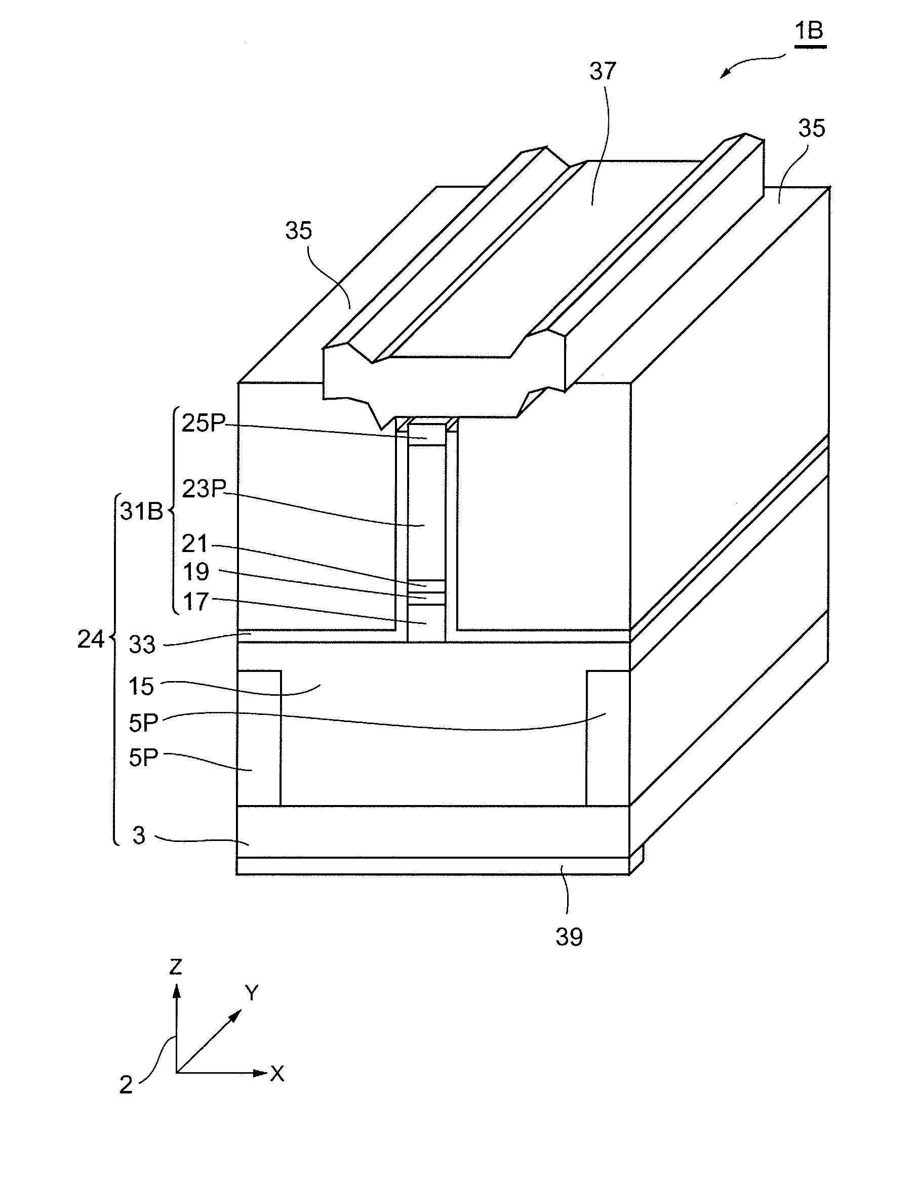
[0041]A method for manufacturing a semiconductor optical modulator and a semiconductor optical modulator according to an embodiment will now be described in detail with reference to the accompanying drawings, where like numerals are used for like elements if possible. The elements in the drawings are not drawn to scale for illustrative purposes.

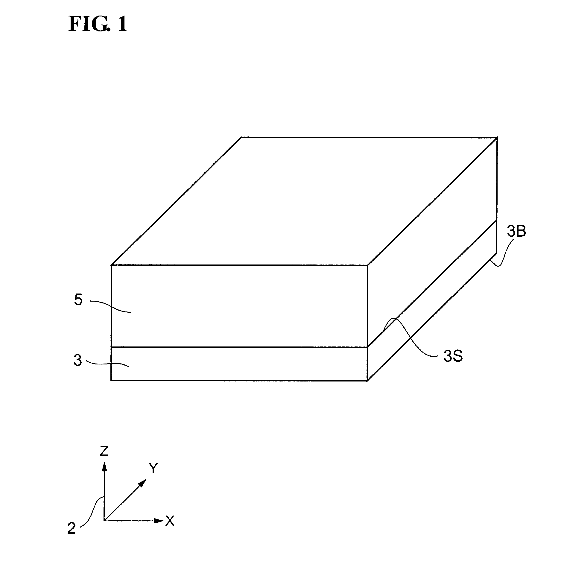
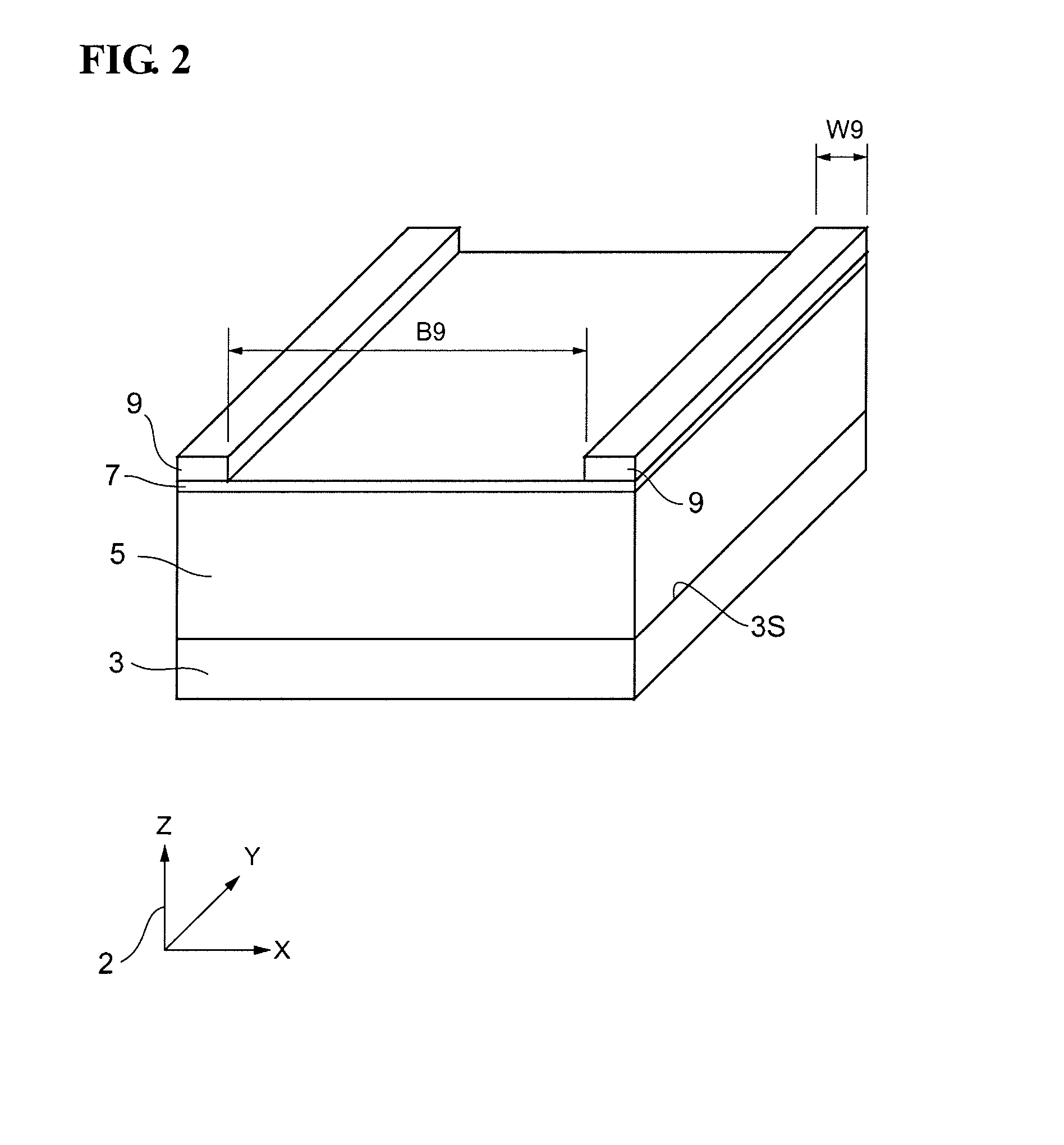
[0042]The method for manufacturing a semiconductor modulator according to this embodiment includes a p-type-semiconductor-layer forming step, a stripe-structure forming step, a buried-layer forming step, a core-layer forming step, an upper-cladding-layer forming step, an optical-waveguide processing step, and an electrode-forming step. FIGS. 1 to 15 are perspective views illustrating the method for manufacturing a semiconductor modulator according to this embodiment. The individual steps will now be described in detail with reference to these figures.

P-Type-Semiconductor-Layer Forming Step

[0043]The method begins with the p-type-semiconductor-...


PUM


Abstract

A method for manufacturing a semiconductor optical modulator includes forming a p-type semiconductor layer on a main surface of a p-type semiconductor substrate; forming a pair of stripe-shaped masks on the p-type semiconductor layer, the stripe-shaped masks extending in a first direction along the main surface of the p-type semiconductor substrate and being spaced apart from each other; simultaneously forming a hole and a pair of stripe structures extending in the first direction by etching the p-type semiconductor layer through the stripe-shaped masks, the pair of stripe structures defining the hole; after removing the stripe-shaped masks, forming a buried layer in the hole; forming a core layer on the buried layer and the stripe structures; and forming an upper cladding layer on the core layer. The buried layer is made of a semiconductor material with a lower optical absorption loss than that of the p-type semiconductor layer.

Description

BACKGROUND OF THE INVENTION[0001]1. Field of the Invention[0002]The present invention relates to methods for manufacturing semiconductor optical modulators and to semiconductor optical modulators.[0003]2. Description of the Related Art[0004]T. H. Stievater et. al., “Enhanced Electro-Optic Phase Shifts in Suspended Waveguides”, OPTICS EXPRESS, 18 Jan. 2010, Vol. 18, No. 2, pp. 885-892 (Ref. 1) discusses a method for manufacturing a semiconductor optical waveguide for a semiconductor optical modulator. In this method for manufacturing an optical waveguide, a p-type AlInAs semiconductor layer is formed on a p-type semiconductor substrate. Then, stacked layers including a core layer are formed on the p-type semiconductor layer. The core layer has a multi-quantum well (MQW) structure. The p-type semiconductor layer and the stacked layers form an optical waveguide structure. Holes are then formed in side surfaces of the optical waveguide structure, and the p-type semiconductor layer is we...

Claims


Application Information

Patent Timeline
IPC IPC(8): G02F1/025H01L21/302
CPCG02F1/025G02F2201/066G02F1/2257
Inventor YAGI, HIDEKI
Owner SUMITOMO ELECTRIC IND LTD
Why Eureka
Try Eureka