Apparatus for conditioning semiconductor chips and test method using the apparatus
Active Publication Date: 2012-12-13
ERS ELECTRONICS
View PDF18 Cites 8 Cited by
Summary
Abstract
Description
Claims
Application Information
AI Technical Summary
This helps you quickly interpret patents by identifying the three key elements:
Problems solved by technology
Method used
Benefits of technology
Benefits of technology
[0006]An object of the present invention is thus to provide a device for conditioning semiconductor chips and a test method using said device which make efficient conditioning and a high throughput possible.
[0010]Therefore, a good thermal connection of the semiconductor chips and also high flexibility is ensured, since the chip bonding pedestal(s) can be easily changed and can be adapted to any chip geometries or chip bonding arrangements.
Problems solved by technology
In this case, it must be ensured that the temperature of the semiconductor chip does not fall below the dew point of the surrounding gaseous medium, since otherwise condensation of the moisture on the surface of the chip or ice forms, which impedes the test measurements or makes them impossible.
In known devices for conditioning semiconductor chips, it has been found to be disadvantageous that loading and unloading the climatic test chamber is time-consuming, condensation problems occur and it is not possible to test a plurality of chips with a high throughput.
Method used
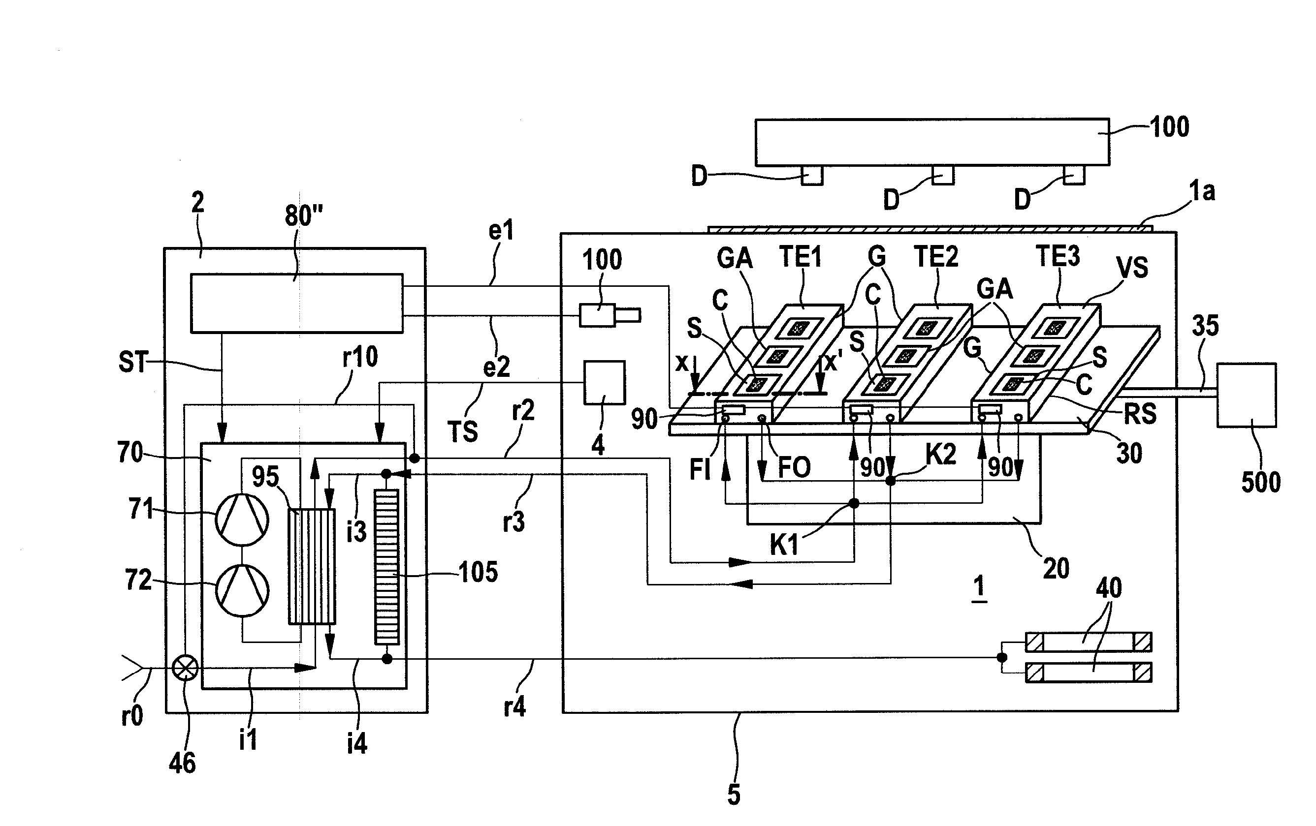
Image
Click on the blue label to locate the original text in one second.
Reading with bidirectional positioning of images and text.
Examples
first embodiment
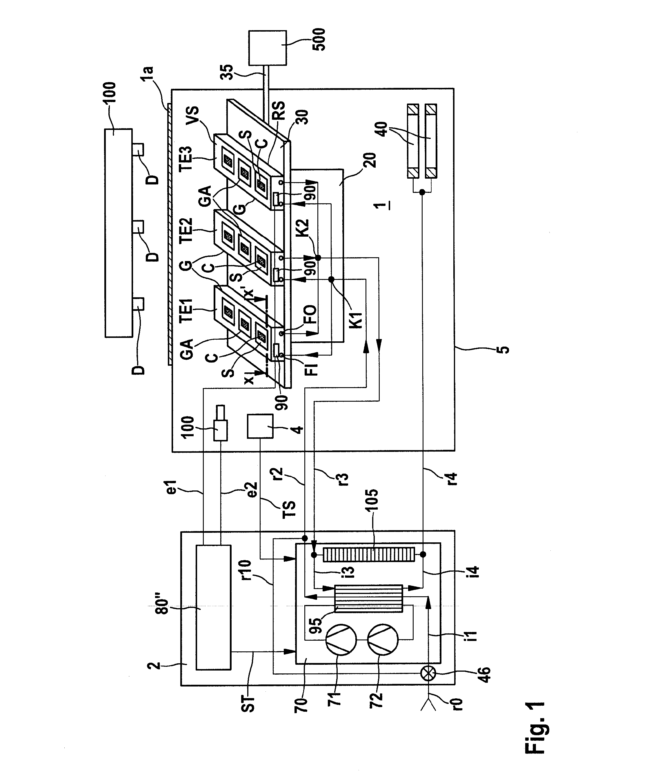
[0021]FIG. 1 is a schematic cross-section of the conditioning device according to the invention.
[0022]In FIG. 1, reference numeral 1 denotes a space in a container 5, in which a temperature control means TE1, TE2, TE3 is provided for receiving a plurality of semiconductor chips C.
[0023]The chip temperature control means TE1, TE2, TE3 consists, in the example shown, of three identical modules TE1, TE2, TE3 which each comprise a base body G, for example made of high-grade steel, which can be flushed with a fluid for temperature control, for example dried air. The base bodies G each comprise a plurality of recesses GA which extend from a front face VS to a rear face RS of the base body G.
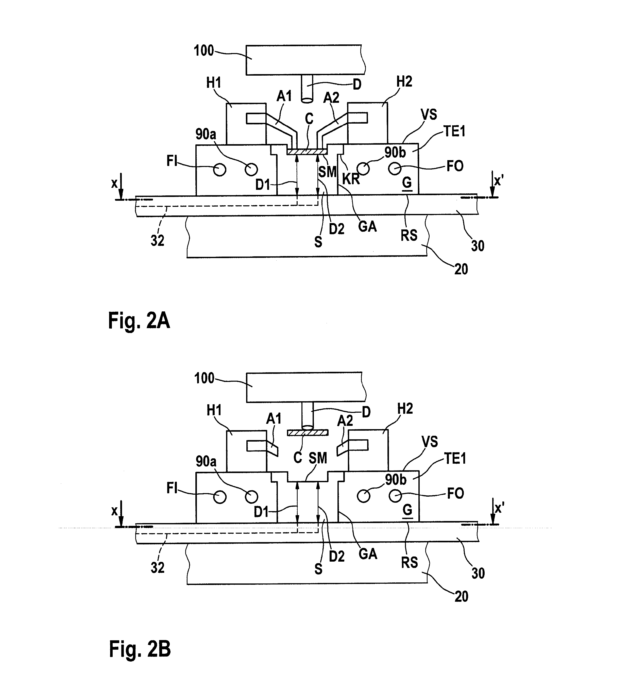
[0024]A plurality of chip bonding pedestals S, for example likewise made of high-grade steel, are respectively inserted into the recesses GA in thermal contact with the base body G. The chip bonding pedestals S have a chip receiving region SM on the front face VS and an insulated wiring means D1, D2 on...
second embodiment
[0051]FIG. 4 is a schematic front view of the temperature control means, the motherboard and the carrier table for representing the conditioning device according to the invention.
[0052]In the second embodiment shown in FIG. 4, the carrier table 20a, on which the motherboard 30 having the temperature control means TE1, TE2, TE3 is provided, can be rotated about an axis A, such that test measurements are possible at various angular positions of the semiconductor chips C. An angle-dependent measurement of this type of semiconductor chips C is necessary in particular for accelerometers in MEMS technology in order to be able to calibrate the chip signals.
[0053]FIG. 5 is a schematic cross-section of the first temperature control means according to a further embodiment of the conditioning device according to the invention.
[0054]FIG. 5 is analogous to FIG. 2A, reference numeral Ht denoting a modified chip holding means. The chip holding means H1′ comprises a holding arm A1′, on the end of w...
PUM
Property
Measurement
Unit
Temperature
aaaaa
aaaaa
Pressure
aaaaa
aaaaa
Mechanical properties
aaaaa
aaaaa
Abstract
The present invention provides a device for conditioning semiconductor chips and a corresponding test method. The device comprises a chiptemperature control means for receiving a semiconductorchip or a plurality of semiconductor chips and comprises a base body which can be flushed with a fluid for temperature control and which comprises a corresponding number of recesses which extend from a front face to a rear face of the base body; a corresponding number of chip bonding pedestals which are inserted, in thermal contact with the base body, into the recesses which comprise a chip receiving region on the front face and a wiring means on the inside which is constructed for supplying electrical signals from and / or to the semiconductor chip inserted in the respective chip receiving region; and a motherboard attached to the rear face in such a way that the wiring means of the chip bonding pedestals is electrically connected to a wiring means of the motherboard.
Description
CROSS-REFERENCE TO RELATED APPLICATION(S)[0001]This application is a Section 371 National Stage Application of International No. PCT / EP2010 / 063975, filed 22 Sep. 2010 and published as WO 2011 / 039087 A1 on 7 Apr. 2011, which claims priority from the DE Patent Application No. 10 2009 045 291.5, filed 2 Oct. 2009, the contents of which are incorporated herein in their entirety for all purposes.FIELD OF THE INVENTION[0002]The present invention relates to a device for conditioning semiconductor chips and a test method using said device.BACKGROUND INFORMATION[0003]Test measurements are known to be carried out on semiconductor chips typically within a temperature range of between −200° C. and +400° C. For temperature control, a semiconductor chip is placed on a bonding pedestal, via which it is connected to an electronic test device, and said bonding pedestal is cooled and / or heated according to the desired temperature and tested in a climatic test chamber together with the semiconductor c...
Claims
Application Information
Patent Timeline
Application Date:The date an application was filed.
Publication Date:The date a patent or application was officially published.
First Publication Date:The earliest publication date of a patent with the same application number.
Issue Date:Publication date of the patent grant document.
PCT Entry Date:The Entry date of PCT National Phase.
Estimated Expiry Date:The statutory expiry date of a patent right according to the Patent Law, and it is the longest term of protection that the patent right can achieve without the termination of the patent right due to other reasons(Term extension factor has been taken into account ).
Invalid Date:Actual expiry date is based on effective date or publication date of legal transaction data of invalid patent.

