Work function tailoring for nonvolatile memory applications

Active Publication Date: 2012-12-13
INTERMOLECULAR
View PDF6 Cites 43 Cited by
  • Summary
  • Abstract
  • Description
  • Claims
  • Application Information

AI Technical Summary

Benefits of technology

[0011]Embodiments of the invention generally relate to a resistive switching nonvolatile memory device having an interface layer structure disposed between at least one of the electrodes and a variable resistance layer formed in the nonvolatile memory device. The resistive switching memory elements may be formed as part of a high-capacity nonvolatile memory integrated circuit, which can be used in various electronic devices, such as digital cameras, mobile telephones, handheld computers, and music players. The resistive switching nonvolatile memory device, comprises a passivation region, an interface coupling region, and / or a variable resistance layer interface region that are configured to adjust the nonvolatile memory device's performance, such as lowering the formed device's switching currents and reducing the device's forming voltage, and reducing the performance variation from one formed device to another.

Problems solved by technology

However, as device dimensions shrink, scaling issues are posing challenges for traditional nonvolatile memory technology.
Although metal oxide (MO) films such as these exhibit bistability, the resistance of these films and / or the ratio of the high-to-low resistance states is (are) often insufficient to be of use within a practical nonvolatile memory device.
Since the variation in the difference between the high and low resistive states is related to the resistance of the resistive switching layer, it is often hard to use a low resistance metal oxide film to form a reliable nonvolatile memory device.
For example, in a nonvolatile memory that has conductive lines formed of a relatively high resistance metal such as tungsten, the resistance of the conductive lines may overwhelm the resistance of the metal oxide resistive switching element.
This may make it difficult or impossible to sense the state of the bistable metal oxide resistive switching element.
Similar issues can arise from integration of the resistive switching memory element with current steering elements, such as diodes and / or resistors.
However, since the power that can be delivered to a circuit containing a series of resistive switching memory elements and current steering elements is typically limited in most conventional nonvolatile memory devices (e.g., CMOS driven devices), it is desirable to form each of the resistive switching memory elements and current steering elements in the circuit so that the voltage drop across each of these elements is small, and thus resistance of the series connected elements does not cause the current to decrease to an undesirable level due to the fixed applied voltage (e.g., ˜2-5 volts).

Method used


Image

  • Work function tailoring for nonvolatile memory applications
  • Work function tailoring for nonvolatile memory applications
  • Work function tailoring for nonvolatile memory applications

Examples


Embodiment Construction

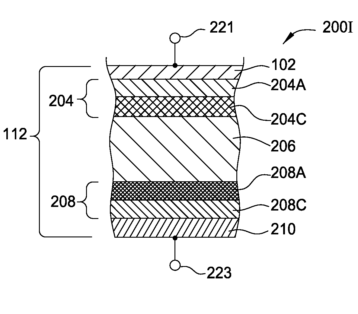
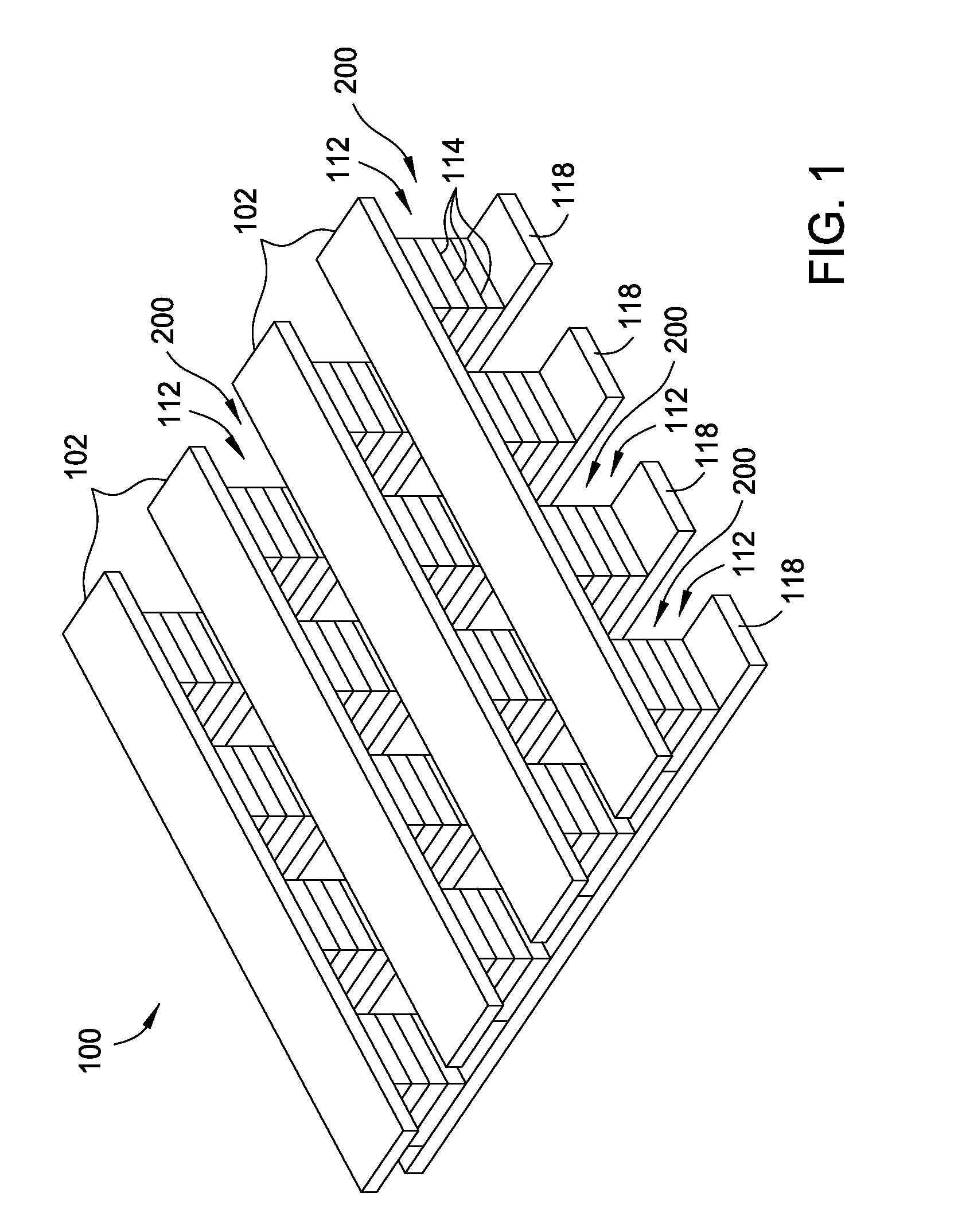
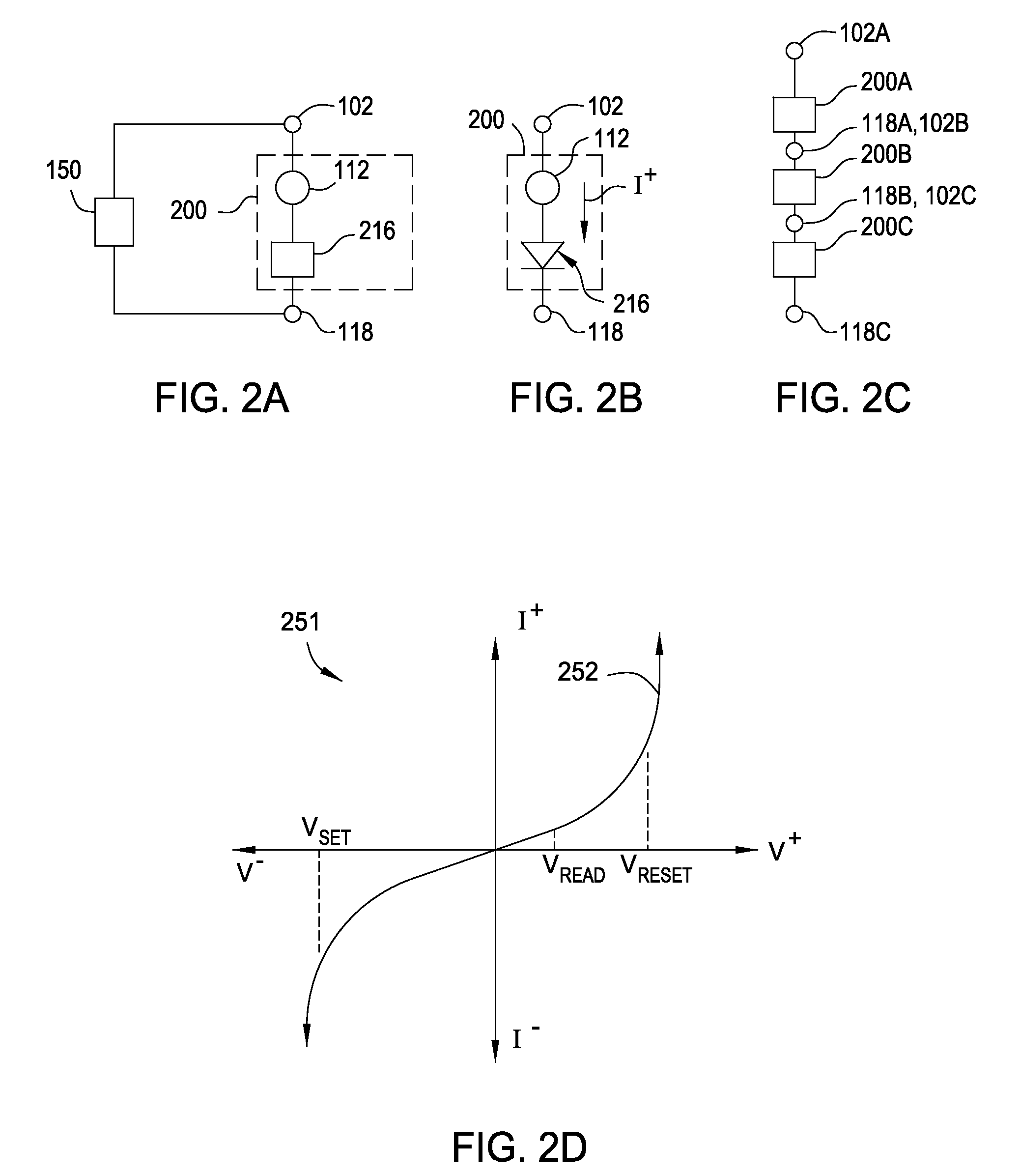
[0035]Embodiments of the invention generally relate to a resistive switching nonvolatile memory device having an interface layer structure disposed between at least one of the electrodes and a variable resistance layer formed in the nonvolatile memory device, and a method of forming the same. Typically, resistive switching memory elements may be formed as part of a high-capacity nonvolatile memory integrated circuit, which can be used in various electronic devices, such as digital cameras, mobile telephones, handheld computers, and music players. In one configuration of the resistive switching nonvolatile memory device, the interface layer structure comprises a passivation region, an interface coupling region, and / or a variable resistance layer interface region that are configured to adjust the nonvolatile memory device's performance, such as lowering the formed device's switching currents and reducing the device's forming voltage, and reducing the performance variation from one for...


PUM


Abstract

Embodiments of the invention generally relate to a resistive switching nonvolatile memory device having an interface layer structure disposed between at least one of the electrodes and a variable resistance layer formed in the nonvolatile memory device, and a method of forming the same. Typically, resistive switching memory elements may be formed as part of a high-capacity nonvolatile memory integrated circuit, which can be used in various electronic devices, such as digital cameras, mobile telephones, handheld computers, and music players. In one configuration of the resistive switching nonvolatile memory device, the interface layer structure comprises a passivation region, an interface coupling region, and / or a variable resistance layer interface region that are configured to adjust the nonvolatile memory device's performance, such as lowering the formed device's switching currents and reducing the device's forming voltage, and reducing the performance variation from one formed device to another.

Description

BACKGROUND OF THE INVENTION[0001]1. Field of the Invention[0002]This invention relates to nonvolatile memory elements, and more particularly, to methods for forming resistive switching memory elements used in nonvolatile memory devices.[0003]2. Description of the Related Art[0004]Nonvolatile memory elements are used in systems in which persistent storage is required. For example, digital cameras use nonvolatile memory cards to store images and digital music players use nonvolatile memory to store audio data. Nonvolatile memory is also used to persistently store data in computer environments.[0005]Nonvolatile memory is often formed using electrically-erasable programmable read only memory (EPROM) technology. This type of nonvolatile memory contains floating gate transistors that can be selectively programmed or erased by application of suitable voltages to their terminals.[0006]As fabrication techniques improve, it is becoming possible to fabricate nonvolatile memory elements with in...

Claims


Application Information

Patent Timeline
IPC IPC(8): H01L47/00
CPCH01L45/04H01L45/146H01L45/1641H01L27/2463H01L45/1608H10B63/80H10N70/235H10N70/20H10N70/25H10N70/801H10N70/826H10N70/8833H10N70/011H10N70/021H10N70/023H10N70/028H10N70/041
Inventor WANG, YUNCHIANG, TONYHASHIM, IMRAN
Owner INTERMOLECULAR
Why Eureka
Try Eureka