
Organic Light Emitting Display Device and Method for Manufacturing the Same

Active Publication Date: 2012-12-13
LG DISPLAY CO LTD
View PDF1 Cites 25 Cited by
  • Summary
  • Abstract
  • Description
  • Claims
  • Application Information

AI Technical Summary

Benefits of technology

[0022]It is one object of the present invention to provide an organic light emitting display device in which permeation of moisture can be prevented, dark defects caused by foreign materials can be improved and lifespan can thus be improved by changing the structure and manufacturing method of thin film encapsulation layer, and a method for manufacturing the same.

Problems solved by technology

However, the organic light emitting display device has disadvantages in that deterioration due to internal factors such as deterioration of electrodes and light emitting layers due to oxygen and deterioration due to reaction between the light emitting layer and the interface, and deterioration due to exterior factors such as moisture, oxygen and UV light readily occur.
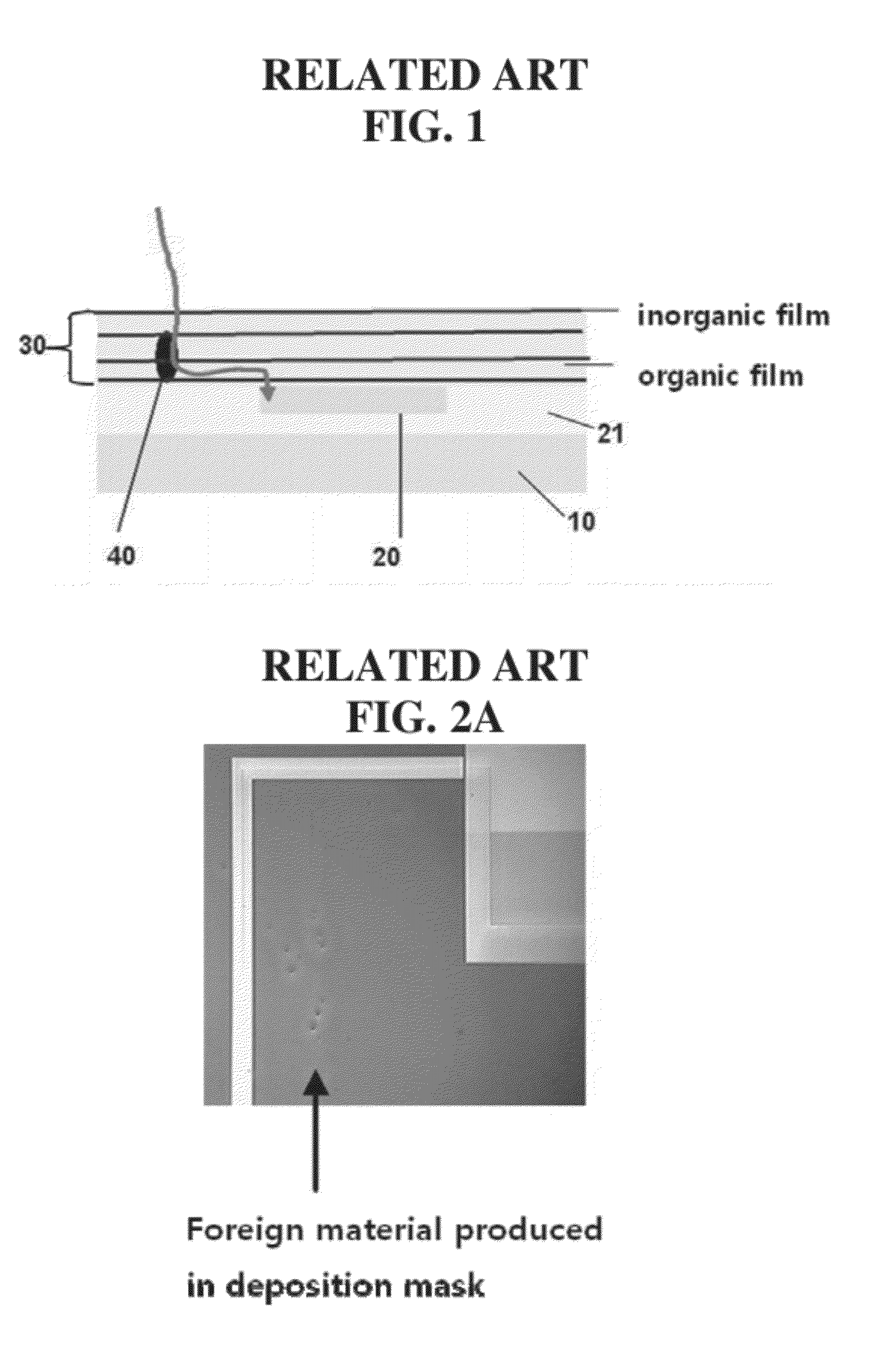
Meanwhile, in a case in which the encapsulation layer 30 is thickly formed, in order to reduce effects of the foreign material 40, disadvantageously, the thickness of the manufactured organic light emitting display device is increased, manufacturing costs increase and yield is deteriorated.
In particular, the organic light emitting element array 20 also causes a secondary problem such as decrease in luminance due to large thickness.
The method for manufacturing an organic light emitting display device of the related art cannot avoid effects of moisture permeation by foreign material or outgassing.
As can be seen from these images, in the edge of the organic light emitting display devices, effects of the foreign material are serious.
However, an increase in thickness of the encapsulation layer in order to reduce effects of the foreign material entails restriction due to deterioration in yield and luminance.
There is a difficulty in forming an encapsulation layer which has a sufficient thickness to block foreign materials.

Method used


Image

  • Organic Light Emitting Display Device and Method for Manufacturing the Same
  • Organic Light Emitting Display Device and Method for Manufacturing the Same
  • Organic Light Emitting Display Device and Method for Manufacturing the Same

Examples


Embodiment Construction

[0043]Reference will now be made in detail to the specific embodiments of the present invention, examples of which are illustrated in the accompanying drawings.

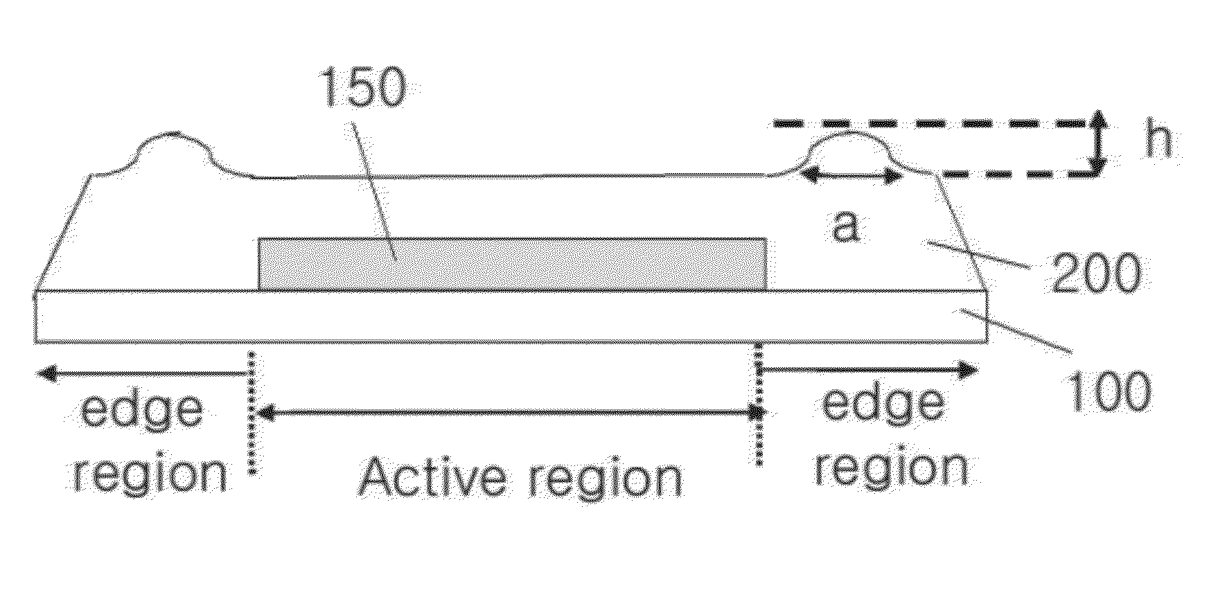
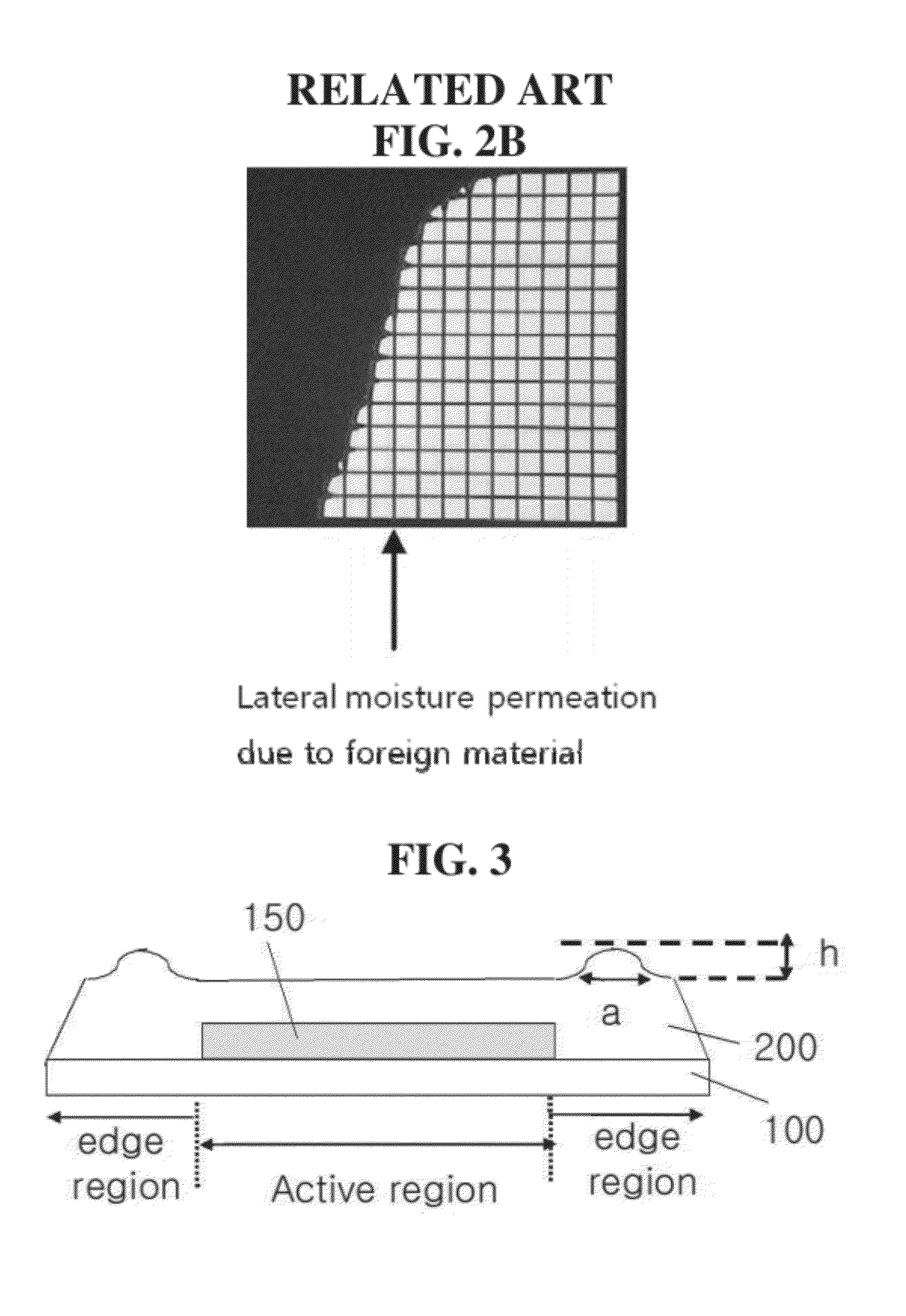
[0044]FIG. 3 is a schematic sectional view illustrating an organic light emitting display device according to the present invention.

[0045]As shown in FIG. 3, the organic light emitting display device of the present invention includes a substrate 100 to define an active region and an edge region, an organic light emitting element array 150 disposed in the active region and a thin film encapsulation layer 200 which covers the organic light emitting element array 150 to protect the organic light emitting element array 150 from the air or moisture of the outside, wherein the edge region of the thin film encapsulation layer 200 is thicker than the active region thereof.

[0046]In particular, the reason for forming the thin film encapsulation layer 200 such that the edge region is thicker than the active region is that, although the ...


PUM


Abstract

Present invention is for an organic light emitting display device in which permeation of exterior moisture can be prevented, dark defects caused by foreign materials can be improved and lifespan can thus be improved by changing the structure and manufacturing method of thin film encapsulation layer, and a method for manufacturing the same, the organic light emitting display device includes the edge region of the thin film encapsulation layer is thicker than the active region thereof and the thin film encapsulation layer includes a plurality of organic film and a plurality of inorganic film, the organic film and the inorganic film being laminated one on top of the other.

Description

CROSS-REFERENCE TO RELATED APPLICATIONS[0001]This application claims priority under 35 U.S.C. 119(a) from Korean Patent Application No. 10-2011-0056347, filed on Jun. 10, 2011, which is hereby incorporated by reference in its entirety.BACKGROUND OF THE INVENTION[0002]1. Field of the Invention[0003]The present invention relates to an organic light emitting display device. More specifically, the present invention relates to an organic light emitting display device in which permeation of exterior moisture can be prevented, dark defects caused by foreign materials can be improved and lifespan can thus be improved by changing the structure and manufacturing method of thin film encapsulation layer, and a method for manufacturing the same.[0004]2. Discussion of the Related Art[0005]Image display devices that realize a variety of information on the screen are core techniques of the information and telecommunication age, which are developed into thinner, lighter weight, portable and high-per...

Claims


Application Information

Patent Timeline
IPC IPC(8): H01J1/70H01J9/00
CPCH01L2251/558H01L51/5256H10K2102/351H10K59/8731C09K15/02C09K15/04H01L23/29H05B33/04H10K50/8445
Inventor KIM, JONG-SUNGKIM, HO-JIN
Owner LG DISPLAY CO LTD
Learn More