Method for manufacturing an arrangement with a component on a carrier substrate, an arrangement and method for manufacturing a semi-finished product, and a semi-finished product

a technology of carrier substrate and manufacturing arrangement, which is applied in the direction of solid-state devices, electrical apparatus construction details, semiconductor devices, etc., can solve the problems of high risk of breaking, affecting the quality of the product, and preventing the use of vacuum handlers,

Active Publication Date: 2012-12-13
MSG LITHOGLAS AG
View PDF3 Cites 12 Cited by
  • Summary
  • Abstract
  • Description
  • Claims
  • Application Information

AI Technical Summary

Benefits of technology

[0015]It is an object of the invention to provide improved technologies for an arrangement with a component on a carrier substrate, in particular an electronic component, which optimizes the possible applications in conjunction with capsulated components, and enables a cost-effective production with high yields. The capsulation is preferably hermetically or quasi-hermetically sealed, in particular with respect to ambient humidity.
[0018]A further aspect of the invention provides an arrangement that is manufactured according to the preceding method and comprises the following features: a carrier substrate, a capsulated component situated on a cover surface of the carrier substrate in a hollow space, and electrical contacts for the component, wherein the hollow space is comprised of spacer elements arranged on the cover surface of the carrier substrate and a cover substrate mounted on the spacer elements, and wherein the spacer elements exhibit a height of about 10 μm to about 300 μm, preferably a height of about 30 μm to about 300 μm, and further preferred a height of about 30 μm to about 100 μm. It was surprisingly found that the method described above enables the reliable and reproducible manufacture of spacer elements with such comparatively low design heights.
[0028]A preferred further development of the invention provides that the one or more recesses are formed in a multistage process, in which another recess is optionally formed in an existing recess. In one configuration, a recess or cavity is effectively introduced in the recess. For example, the additional recess can be formed on the floor of the previously generated recess, resulting in a larger depth overall. The multistage process is performed in one embodiment by means of masking, which makes it possible to mask portions of a first recess once it has been formed, so as to generate the additional recess in the existing recess. Examples of possible masking technologies include the use of a (separate) metal mask, through which evaporating can take place, and / or the application of a photoresist mask on the substrate. It can also be provided that a multistage process be developed to generate recesses or cavities of varying scope in several sequential procedural steps as an alternative or supplement to manufacturing the additional recess in the existing recess. The shadow mask technology can also be used to this end, making it possible to shadow regions within the individual procedural steps.

Problems solved by technology

The known method has disadvantages when given the objective of manufacturing thin spacers or large quantities.
The thin frame wafers required by the known method are fragile, and run a high risk of breaking while being applied to the cover plate wafer.
In addition, the frame wafers exhibit continuous openings, which preclude any automatic handling with vacuum handlers commonly encountered in the industry.
While this problem can be circumvented by means of temporarily bonded carrier wafers for some applications, doing so results in additional material usage and additional procedural steps, and hence in elevated costs.

Method used


Image

  • Method for manufacturing an arrangement with a component on a carrier substrate, an arrangement and method for manufacturing a semi-finished product, and a semi-finished product
  • Method for manufacturing an arrangement with a component on a carrier substrate, an arrangement and method for manufacturing a semi-finished product, and a semi-finished product
  • Method for manufacturing an arrangement with a component on a carrier substrate, an arrangement and method for manufacturing a semi-finished product, and a semi-finished product

Examples


Embodiment Construction

[0051]The invention will be described in greater detail below based on preferred exemplary embodiments, with reference to the figures of a drawing. Shown on:

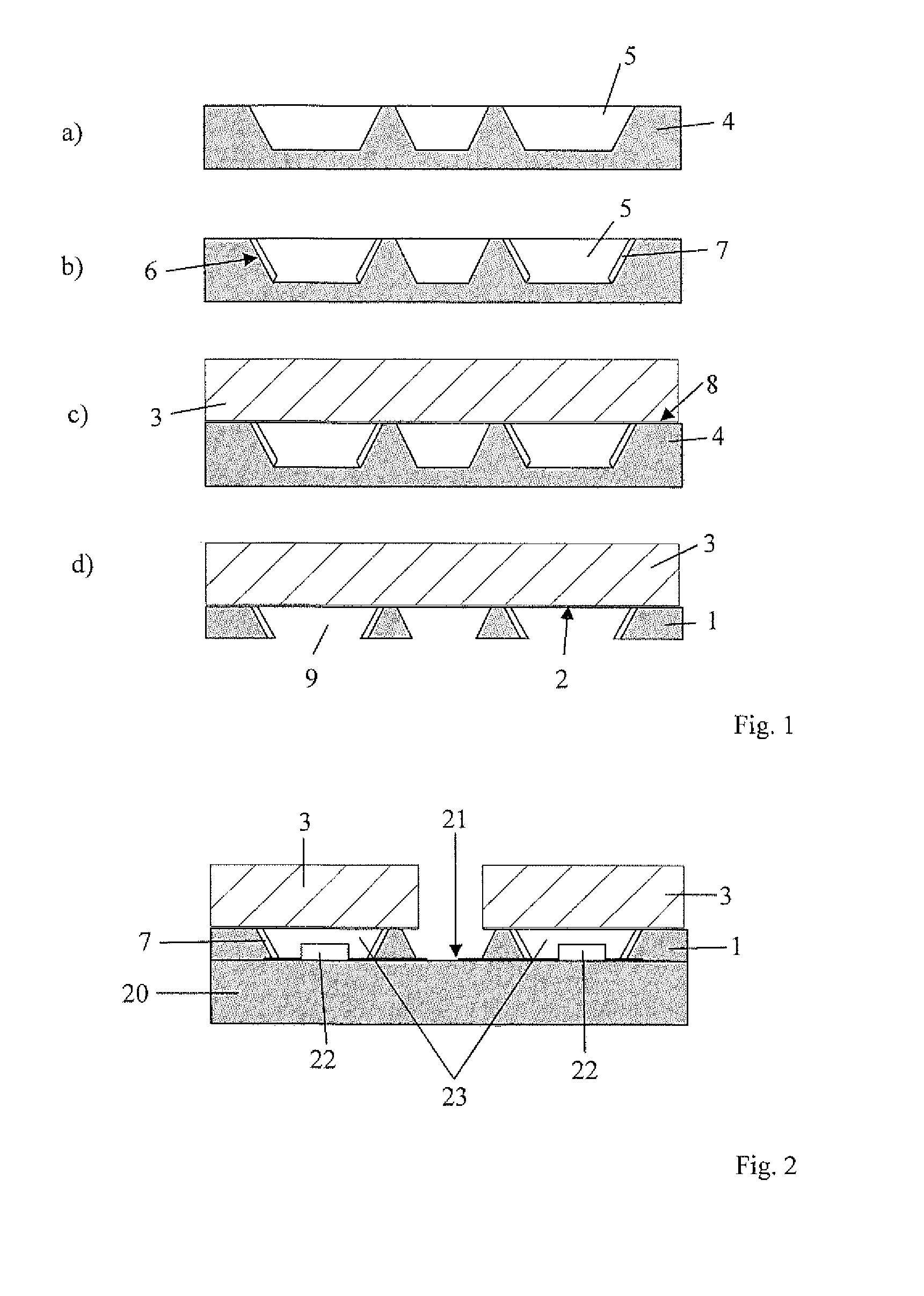
[0052]FIG. 1 is a diagrammatic view for explaining several procedural steps involved in manufacturing spacer elements,

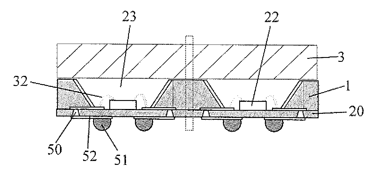
[0053]FIG. 2 is a diagrammatic view of an arrangement in which the components are each arranged in a hollow space on a carrier substrate,

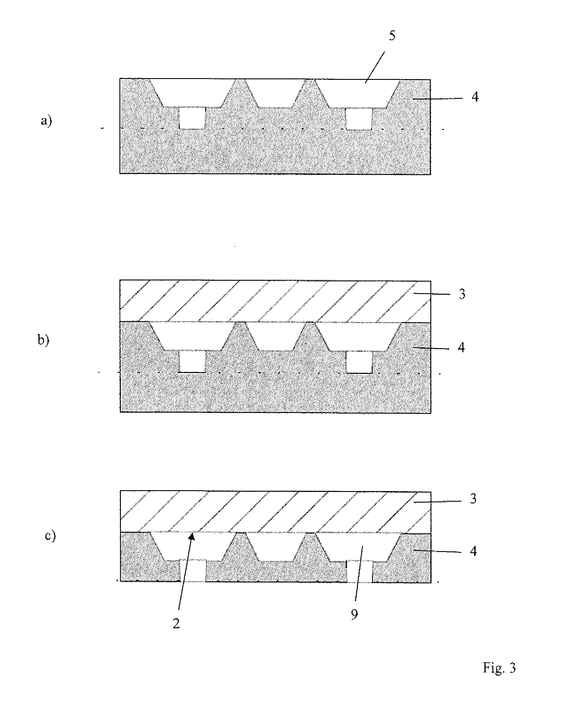
[0054]FIG. 3 is a diagrammatic view for explaining several procedural steps involved in manufacturing spacer elements according to another embodiment, in which cavities are fabricated in differing configurations,

[0055]FIG. 4 is a diagrammatic view for explaining several procedural steps involved in manufacturing spacer elements according to a further embodiment, in which back thinning is performed by means of a masking technology,

[0056]FIG. 5 is a diagrammatic view of an arrangement in which a component is arranged on a carrier substrate in a hollow space, wherein spacer element...


PUM

PropertyMeasurementUnit
heightaaaaaaaaaa
heightaaaaaaaaaa
heightaaaaaaaaaa

Abstract

The invention relates to a method for manufacturing an arrangement with a component on a carrier substrate, wherein the method encompasses the following steps: Manufacturing spacer elements on the rear side of a cover substrate, arranging a component on a cover surface of a carrier substrate, and arranging the spacer elements formed on the carrier substrate so as to situate the component in the at least one hollow space and close the latter. In addition, the invention relates to an arrangement, a method for manufacturing a semi-finished product for a component arrangement, as well as a semi-finished product for a component arrangement.

Description

[0001]The invention relates to a method for manufacturing an arrangement with a component on a carrier substrate, an arrangement and method for manufacturing a semi-finished product, and a semi-finished product.BACKGROUND OF THE INVENTION[0002]Known in the art in particular in conjunction with electronic components are arrangements in which the electronic component is applied to a carrier substrate, for example a semiconductor material. Various proposals have been made for arrangements in which the component is arranged in a hollow space, which is also referred to as encapsulation or capsulation.[0003]Known from document U.S. Pat. No. 6,932,519 B2 is an arrangement in which an optical component is arranged in a recess or cavity on the carrier substrate. Spacer elements arranged laterally from the recess on the cover surface of the carrier substrate are used to space a cover substrate apart from the carrier substrate to form the hollow space. The recess in the carrier substrate is fo...

Claims


Application Information

Patent Timeline
Patent Type & Authority Applications(United States)
IPC IPC(8): H05K7/02H05K13/04
CPCH01L31/0203H01L33/005H01L33/483H01L33/58H01L33/60Y10T29/49002H01L2924/09701H01L2224/48091H01L2924/01322H01L2924/01068H01L2924/00014H01L33/48H01L24/97H01L2224/48227H01L2924/1815Y10T29/49128Y10T29/4913Y10T29/49146Y10T29/49155Y10T29/49169H01L33/52H01L31/02005H01L31/0232H01L33/62
Inventor LEIB, JURGENMAUS, SIMONHANSEN, ULLI
Owner MSG LITHOGLAS AG
Why Eureka
Try Eureka