Clamped bit line read circuit

a bit line and read circuit technology, applied in the field of digital memory circuits, can solve the problems of low switching margin, low reliability of conventional storage cells, and unstable read operations, and achieve the effects of less leakage, less dynamic power dissipation, and reduced static power

Active Publication Date: 2012-12-20
NVIDIA CORP
View PDF2 Cites 10 Cited by
  • Summary
  • Abstract
  • Description
  • Claims
  • Application Information

AI Technical Summary

Benefits of technology

[0014]One advantage of the disclosed circuit is that the bit lines do not need to be precharged prior to each read operation. Therefore, the dynamic power dissipation is reduced significantly compared with memory arrays using storage cells that need to be precharged prior to each read operation. Static power is also significantly reduced becau...

Problems solved by technology

However, as the process technology shrinks, the reliability of conventional storage cells is reduced due to variations in the process and low operating voltages.
One problem that results fr...

Method used


Image

  • Clamped bit line read circuit
  • Clamped bit line read circuit
  • Clamped bit line read circuit

Examples


Embodiment Construction

[0031]In the following description, numerous specific details are set forth to provide a more thorough understanding of the present invention. However, it will be apparent to one of skill in the art that the present invention may be practiced without one or more of these specific details. In other instances, well-known features have not been described in order to avoid obscuring the present invention.

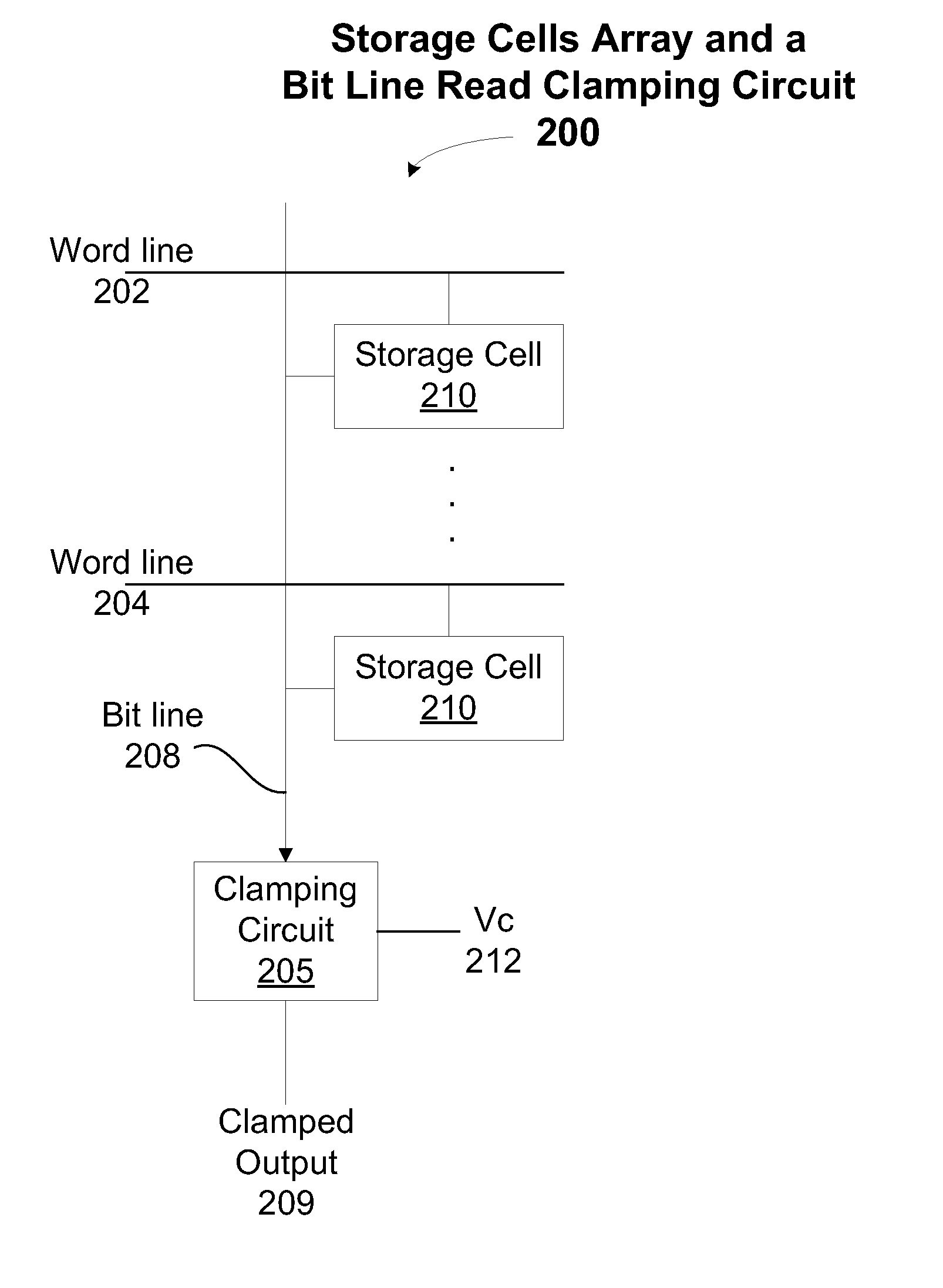
[0032]FIG. 2A illustrates a diagram of a storage cells of a memory array that are coupled to a bit line read clamping circuit 200, according to one embodiment of the invention. A clamping circuit 205 maintains the bit line 208 at a nearly constant clamp voltage of Vc 212. When at least one inverter is used in the feedback path (as shown in FIGS. 3A and 3B), the nearly constant clamp voltage of Vc 212 is Vinv, the threshold voltage of the inverter, the voltage at which the input and output voltage of the inverter are equal. In one embodiment, the nearly constant clamp voltage equals half...


PUM


Abstract

One embodiment of the present invention sets forth a clamping circuit that is used to maintain a bit line of a storage cell in a memory array at a nearly constant clamp voltage. During read operations the bit line is pulled high or low from the clamp voltage by the storage cell and a change in current on the bit line is converted by the clamping circuit to produce an amplified voltage that may be sampled to read a value stored in the storage cell. The clamping circuit maintains the nearly constant clamp voltage on the bit line. Clamping the bit line to the nearly constant clamp voltage reduces the occurrence of read disturb faults. Additionally, the clamping circuit functions with a variety of storage cells and does not require that the bit lines be precharged prior to each read operation.

Description

BACKGROUND OF THE INVENTION[0001]1. Field of the Invention[0002]The present invention generally relates to digital memory circuits and more specifically to a clamped bit line read circuit.[0003]2. Description of the Related Art[0004]As the process technology enables the fabrication of transistors having smaller dimensions and the density of semiconductor memory devices increases. However, as the process technology shrinks, the reliability of conventional storage cells is reduced due to variations in the process and low operating voltages.[0005]FIG. 1A illustrates a conventional 6 transistor storage cell 100 configured in a memory array, according to the prior art. The 6 transistor storage cell 100 is a conventional static random access memory (SRAM) cell that includes four NMOS transistors and two PMOS transistors. A word line 102, coupled to the gates of two pass transistors may be enabled to read from or write to a storage circuit formed by cross-coupled inverters. The word line 1...

Claims


Application Information

Patent Timeline
IPC IPC(8): G11C7/12G11C7/10
CPCG11C7/12G11C11/412G11C11/419
Inventor DALLY, WILLIAM J.POULTON, JOHN W.
Owner NVIDIA CORP
Why Eureka
Try Eureka