

Transparent LED wafer module and method for manufacturing same
- Summary
- Abstract
- Description
- Claims
- Application Information
AI Technical Summary
Benefits of technology
Problems solved by technology
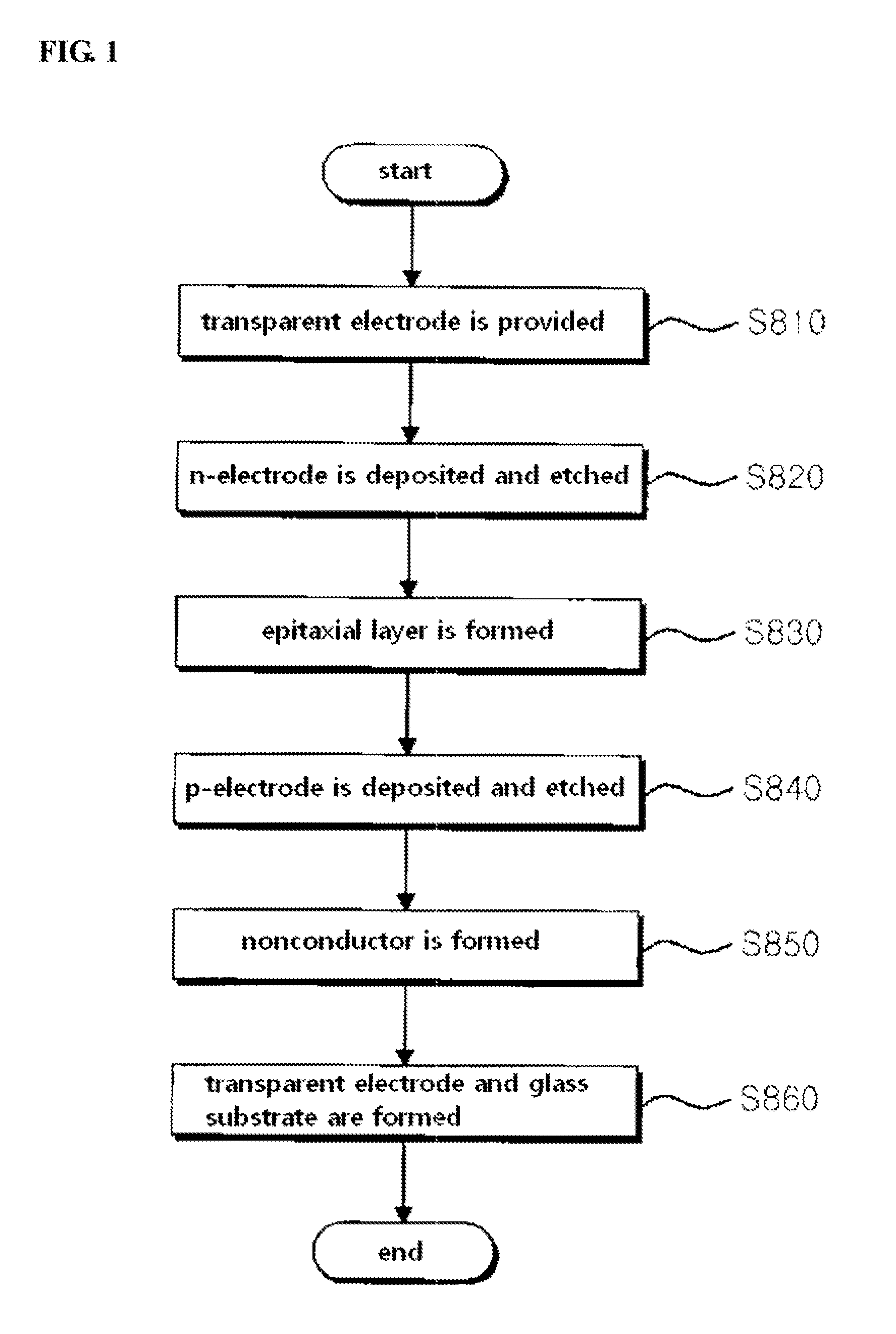
Method used
Image

Examples
Embodiment Construction
Technical Problem
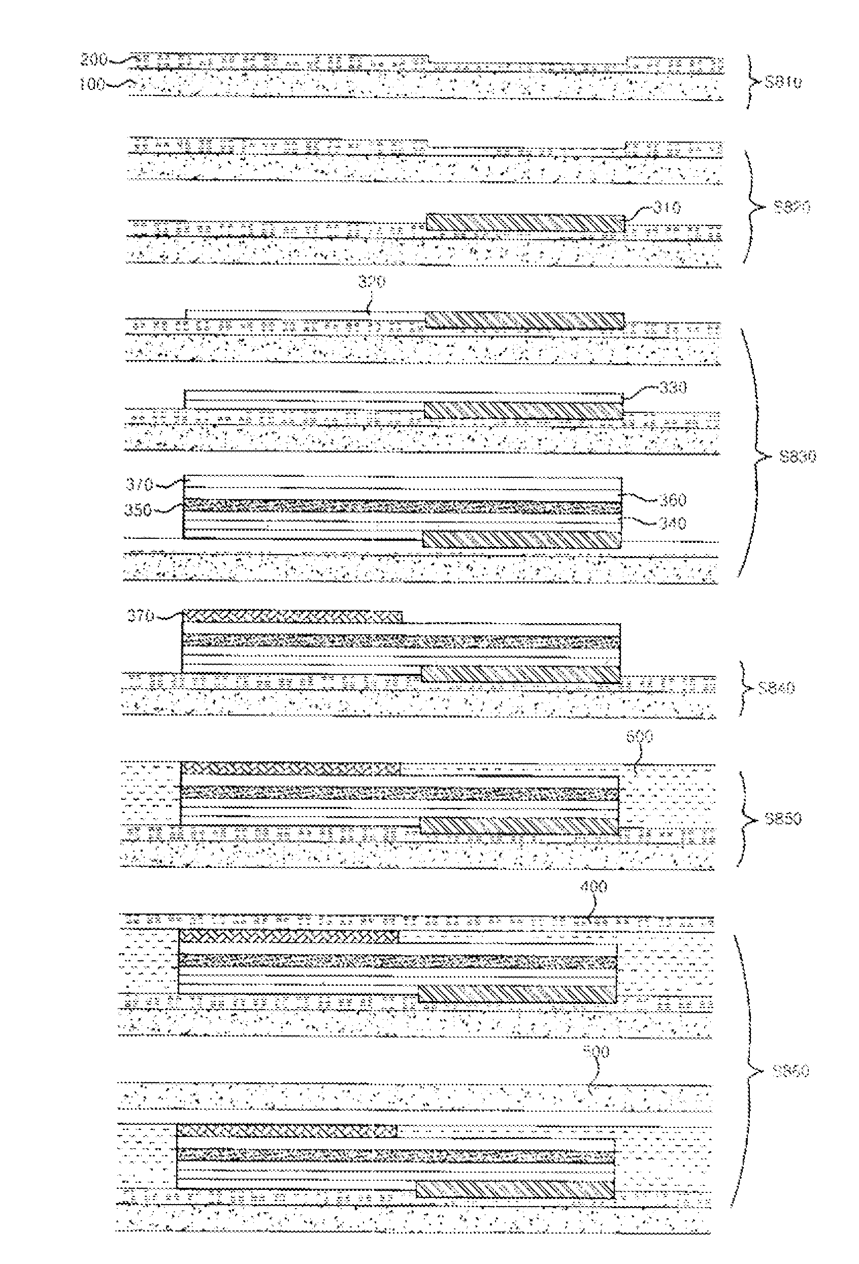
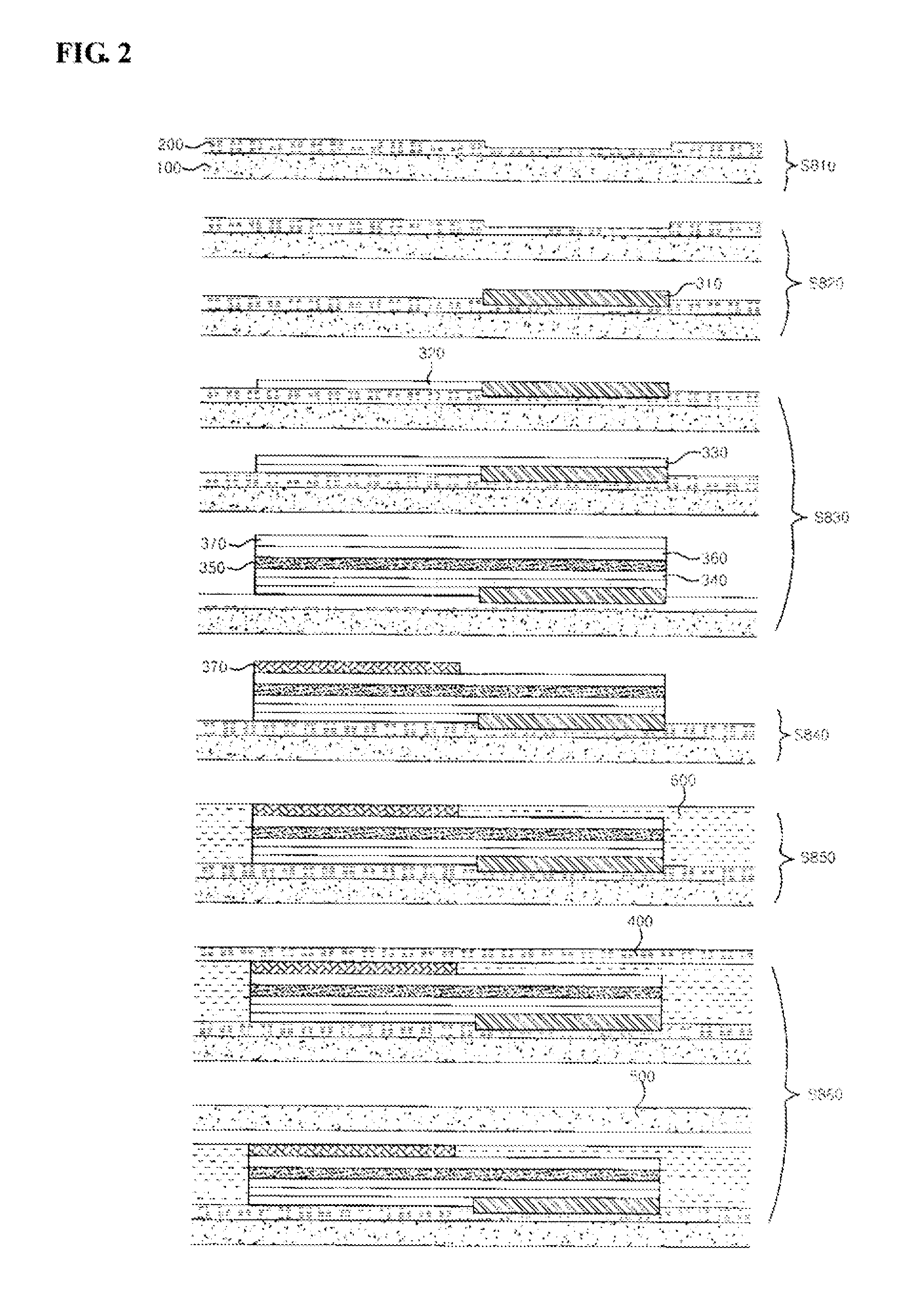
[0012]Therefore, the present invention has been made in view of the above-mentioned problems, and an aspect of the present invention is to provide a transparent LED wafer module and a method for manufacturing the same, in which in an epitaxial process, an LED device is grown on a wafer made of a transparent material, wherein both surfaces of the LED device are entirely grown on the transparent material, and then a layered structure is formed to secure an amount of light. Further, in the method, it is possible to complete the LED module in the epitaxial process, to reduce process steps, and to secure in actuality a high amount of light.
[0013]An object of the present invention is to provide a transparent LED wafer module and a method for manufacturing the same, in which in a LED chip device, multiple epitaxial structures are grown on a transparent glass substrate, wherein firstly, only minimum epitaxial structures are grown so that heat emitted from the epitaxial stru...
PUM
 Abstract
Description
Claims
Application Information