

Hybrid Impedance Compensation in a Buffer Circuit
a buffer circuit and impedance compensation technology, applied in the field of hybrid impedance compensation in buffer circuits, can solve the problems of reducing the efficiency of ic layout area, increasing design complexity, and reducing the relative error (impedance mismatch) between pull-up and pull-down impedances, so as to achieve significant reduction of design complexity and layout area penalty
- Summary
- Abstract
- Description
- Claims
- Application Information
AI Technical Summary
Problems solved by technology
Method used
Image

Examples
Embodiment Construction
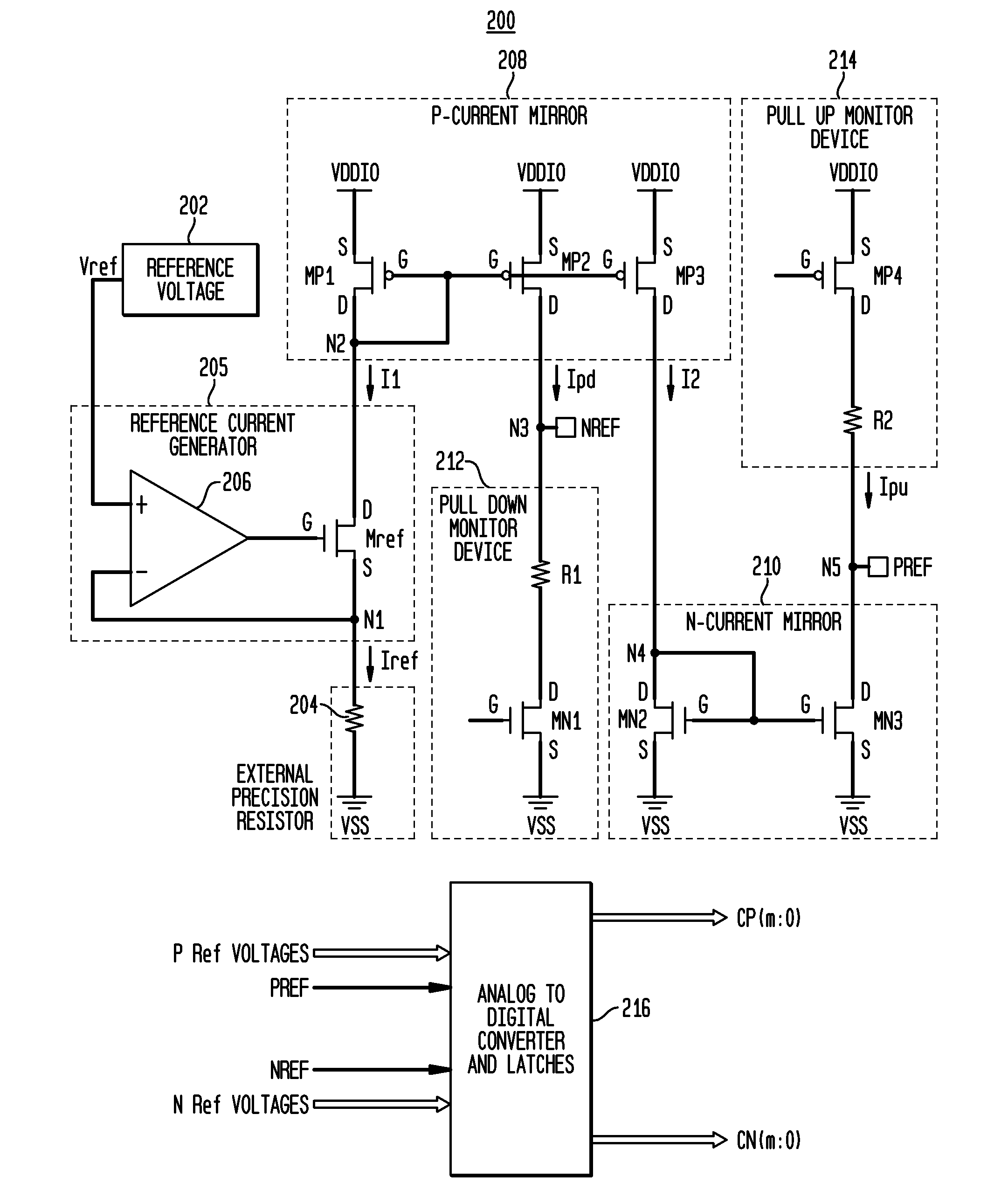
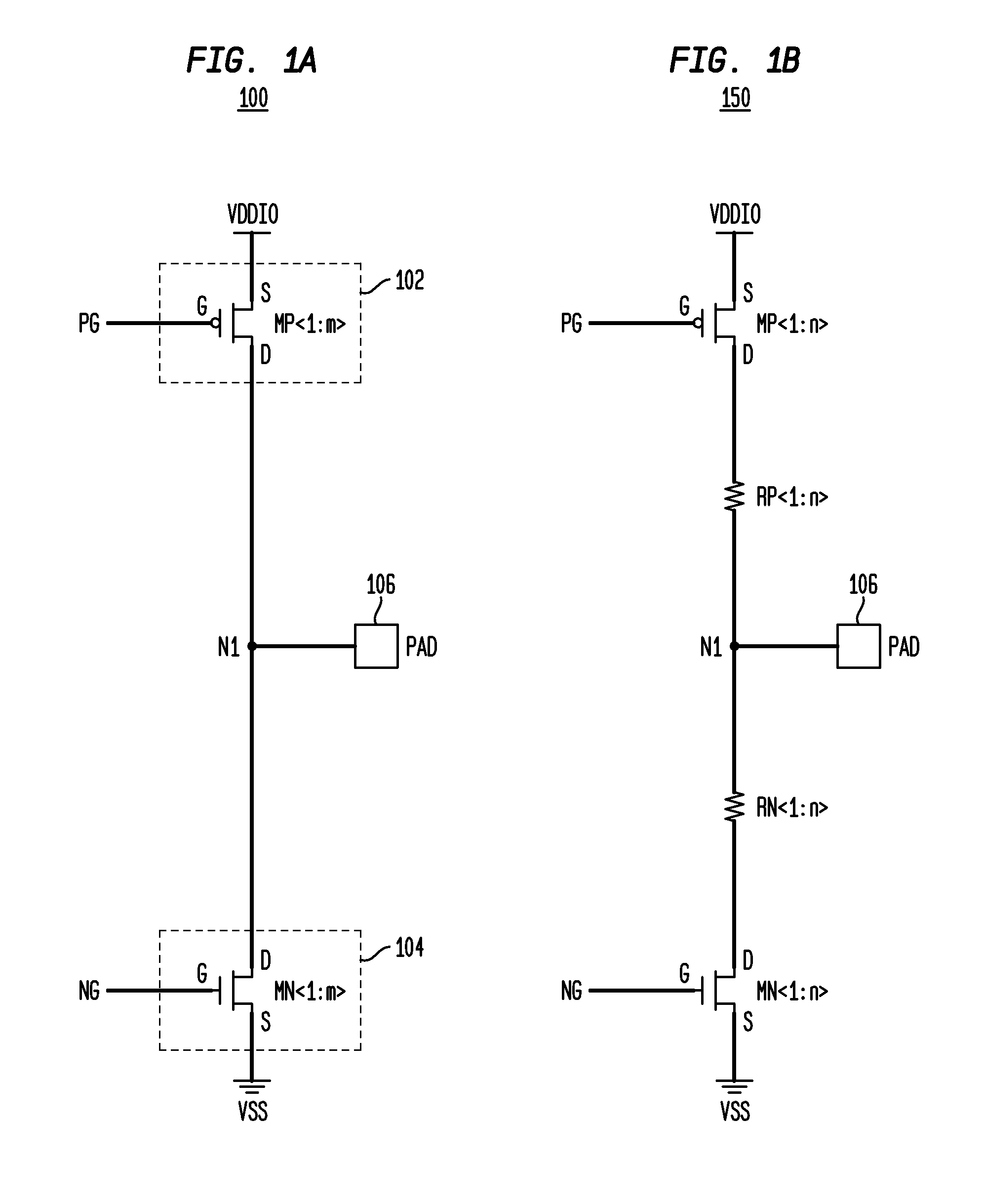
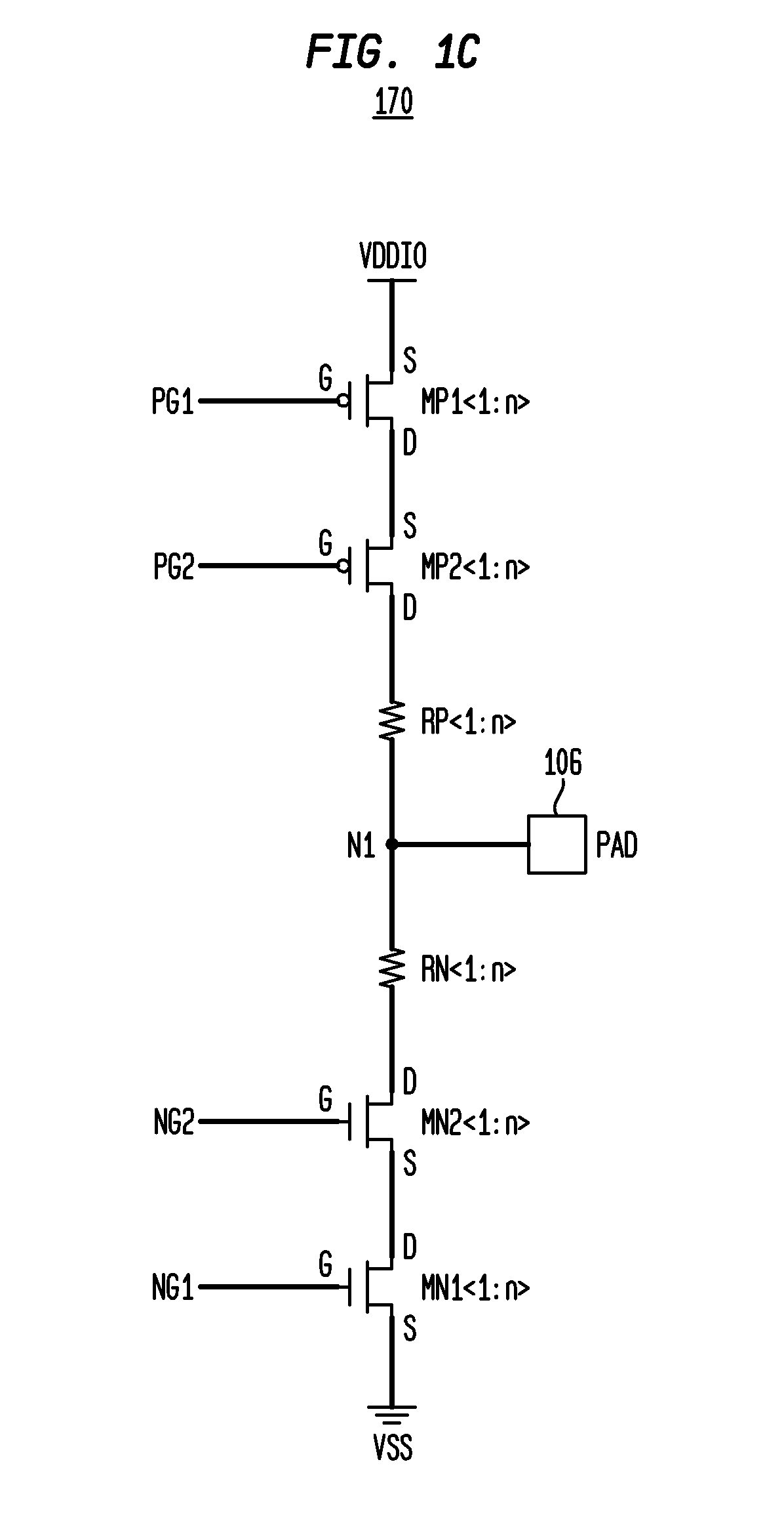
[0021]The present invention, according to aspects thereof, will be described herein in the context of illustrative compensation circuits adapted to control a variation in output impedance and to control a relative variation between pull-up and pull-down impedances of a buffer circuit over variations in PVT conditions to which the buffer circuit may be subjected. It should be understood, however, that the present invention is not limited to these or any other particular circuit arrangements. Rather, the invention is more generally applicable to techniques for compensating a buffer circuit in such a way that design complexity and layout area penalty is significantly reduced compared to conventional buffer design approaches, among other advantages. To accomplish this, embodiments of the invention utilize a hybrid compensation approach whereby a status of both pull-up and pull-down impedances are combined to generate a single set of compensation bits that are applied to both pull-up and...
PUM
 Abstract
Description
Claims
Application Information