Nanostructure and manufacturing method thereof, and solar cell including the same

a manufacturing method and solar cell technology, applied in the direction of sustainable manufacturing/processing, final product manufacturing, transportation and packaging, etc., can solve the problems of decreasing energy conversion efficiency, achieve the effect of improving reducing the loss of electrons generated by light reaction, and increasing the specific surface area for absorbing ligh

Inactive Publication Date: 2013-01-03
KOREA ADVANCED INST OF SCI & TECH
View PDF4 Cites 11 Cited by
  • Summary
  • Abstract
  • Description
  • Claims
  • Application Information

AI Technical Summary

Benefits of technology

[0025]According to the present invention, a nanostructure includes a plurality of nanowires formed at predetermined intervals on a substrate and a plurality of nanobranches enclosing the side surface of the nanowires, thereby increasing the specific surface area for absorbing light, and resultantly the light absorption ratio may be improved.
[0026]Further, the dye sensitized solar cell having the photoelectrode including the nanostructure acco...

Problems solved by technology

However, the porous photoelectrode made of titanium oxide (TiO2) has a poor depletion layer such that an energy loss due to hole and electr...

Method used


Image

  • Nanostructure and manufacturing method thereof, and solar cell including the same
  • Nanostructure and manufacturing method thereof, and solar cell including the same
  • Nanostructure and manufacturing method thereof, and solar cell including the same

Examples


Embodiment Construction

[0034]The present invention will be described more fully hereinafter with reference to the accompanying drawings, in which exemplary embodiments of the invention are shown. As those skilled in the art would realize, the described embodiments may be modified in various different ways, all without departing from the spirit or scope of the present invention.

[0035]Descriptions of parts not related to the present invention are omitted, and like reference numerals designate like elements throughout the specification.

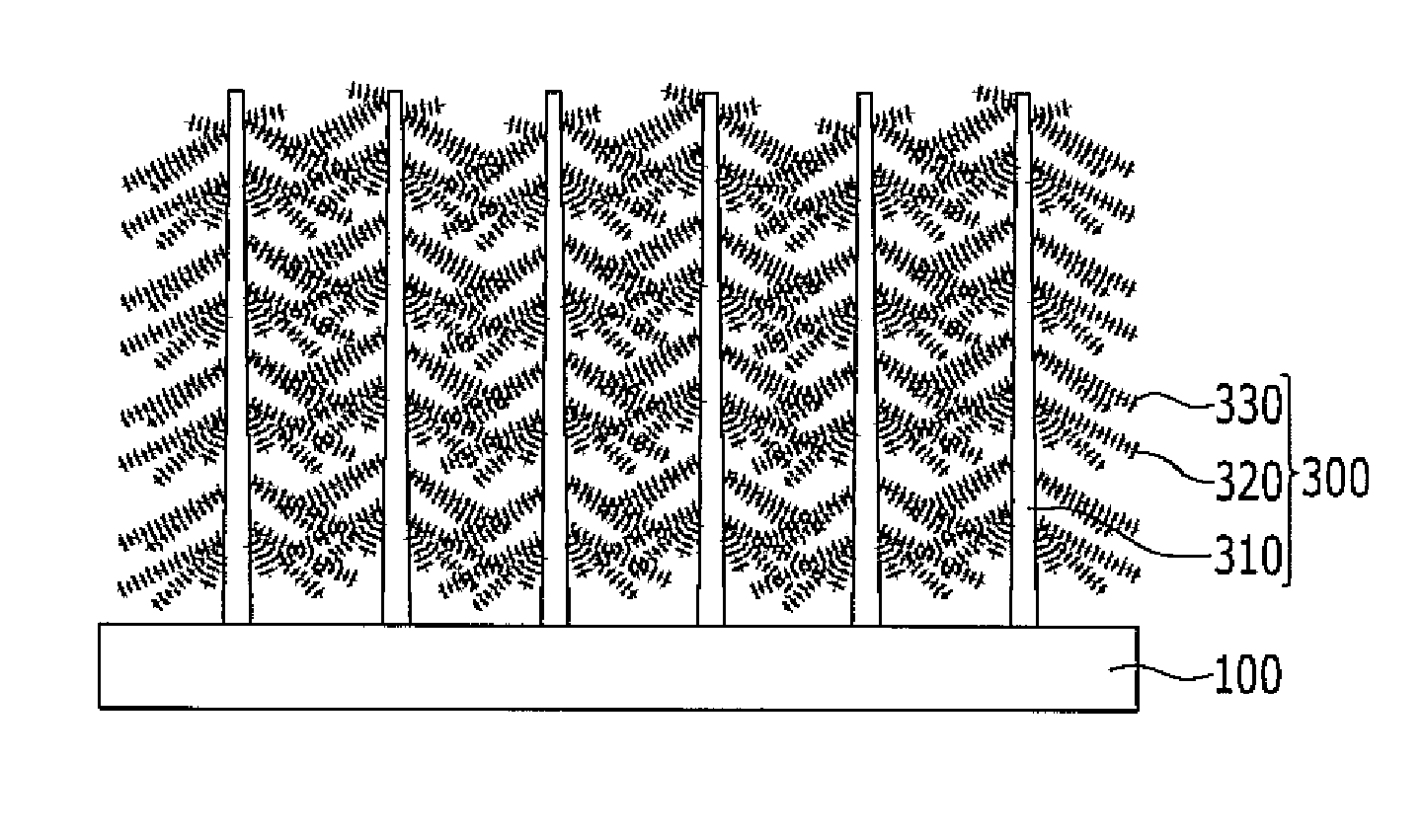
[0036]A nanostructure 300 according to an exemplary embodiment of the present invention will now be described with reference to FIG. 1.

[0037]FIG. 1 is a side view of the nanostructure 300 according to an exemplary embodiment of the present invention.

[0038]As shown in FIG. 1, the nanostructure 300 according to an exemplary embodiment of the present invention includes a plurality of nanowires 310 formed at a predetermined interval on a substrate 100, a plurality of nanobranches ...


PUM


Abstract

A manufacturing method of a nanostructure according to an exemplary embodiment of the present invention includes: adhering a plurality of first nanoparticles on a substrate to form a nanoseed layer; growing the nanoseed layer on the substrate to form a plurality of nanowires; adhering a plurality of second nanoparticles to the side surface of the nanowires to form a nanoshell layer; and growing the nanoshell layer to form a plurality of nanobranches.

Description

CROSS-REFERENCE TO RELATED APPLICATION[0001]This application claims priority to and the benefit of Korean Patent Application No. 10-2011-0063970 filed in the Korean Intellectual Property Office on Jun. 29, 2011, the entire contents of which are incorporated herein by reference.BACKGROUND OF THE INVENTION[0002](a) Field of the Invention[0003]The present invention relates to a nanostructure, a manufacturing method thereof, and a solar cell including the same.[0004](b) Description of the Related Art[0005]In general, a nanostructure has various functionalities in electrical, electronic, optical, and engineering applications such that research thereof has been actively performed as a core element in application fields such as energy, displays, sensors, and bionics.[0006]Particularly, a metal oxide such as TiO2 and ZnO may have a shape of a nanoparticle, a nanowire, or a nanotube, and a nanostructure of a desired shape and structure for various applications may be formed as the importance...

Claims


Application Information

Patent Timeline
IPC IPC(8): H01L31/0224B05D3/00B05D1/38B32B5/02B05D5/00B82Y99/00
CPCB82Y30/00H01G9/204Y10T428/24074Y02E10/542Y02E10/549H01L51/4233Y02P70/50H10K30/152H01L31/04H01L31/18
Inventor KO, SEUNG HWANKANG, HYUN WOOKYEO, JUNYEOBHONG, SUKJOONSUNG, HYUNG JIN
Owner KOREA ADVANCED INST OF SCI & TECH
Why Eureka
Try Eureka