Trench junction barrier schottky structure with enhanced contact area integrated with a mosfet

a mosfet and contact area technology, applied in the field of mosfet technology, can solve the problems of limited shrinking capability and power loss of future devices, and achieve the effect of improving the performance and efficiency of schottky diodes and increasing the contact area

Inactive Publication Date: 2013-01-03
SINOPOWER SEMICON
View PDF2 Cites 11 Cited by
  • Summary
  • Abstract
  • Description
  • Claims
  • Application Information

AI Technical Summary

Benefits of technology

[0006]An object of this invention is to provide a Schottky diode structure to increase the contact area at a Schottky junction between a Schottky barrier metal and a semiconductor substrate. The

Problems solved by technology

In operating, the lower side (LS) MOSFET usually requires longer time to switch from off state to on state; and, during such time period, a body diode may turn on by a higher voltage at the drain than at the source electrode, which will cause power losses in the high side MOSFET by the current flowing from the drain electrode through the body

Method used


Image

  • Trench junction barrier schottky structure with enhanced contact area integrated with a mosfet
  • Trench junction barrier schottky structure with enhanced contact area integrated with a mosfet
  • Trench junction barrier schottky structure with enhanced contact area integrated with a mosfet

Examples


Embodiment Construction

[0022]The invention will now be described in greater detail with preferred embodiment and illustrations attached. Nevertheless, it should be recognized that the preferred embodiments of the invention are only for illustrating. Besides the preferred embodiments mentioned here, this present invention can be practiced in a wide range of other embodiments besides those explicitly described, and the scope of the present invention is expressly not limited expect as specified in the accompanying claims.

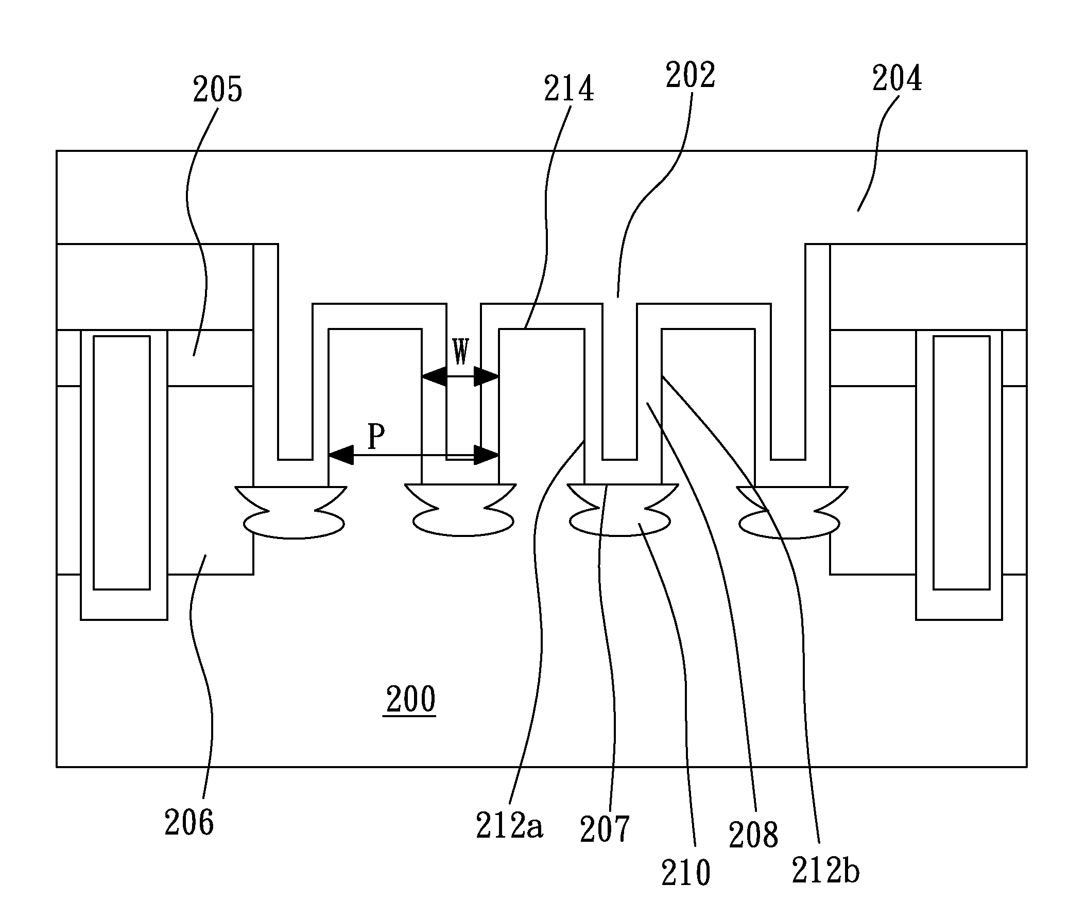
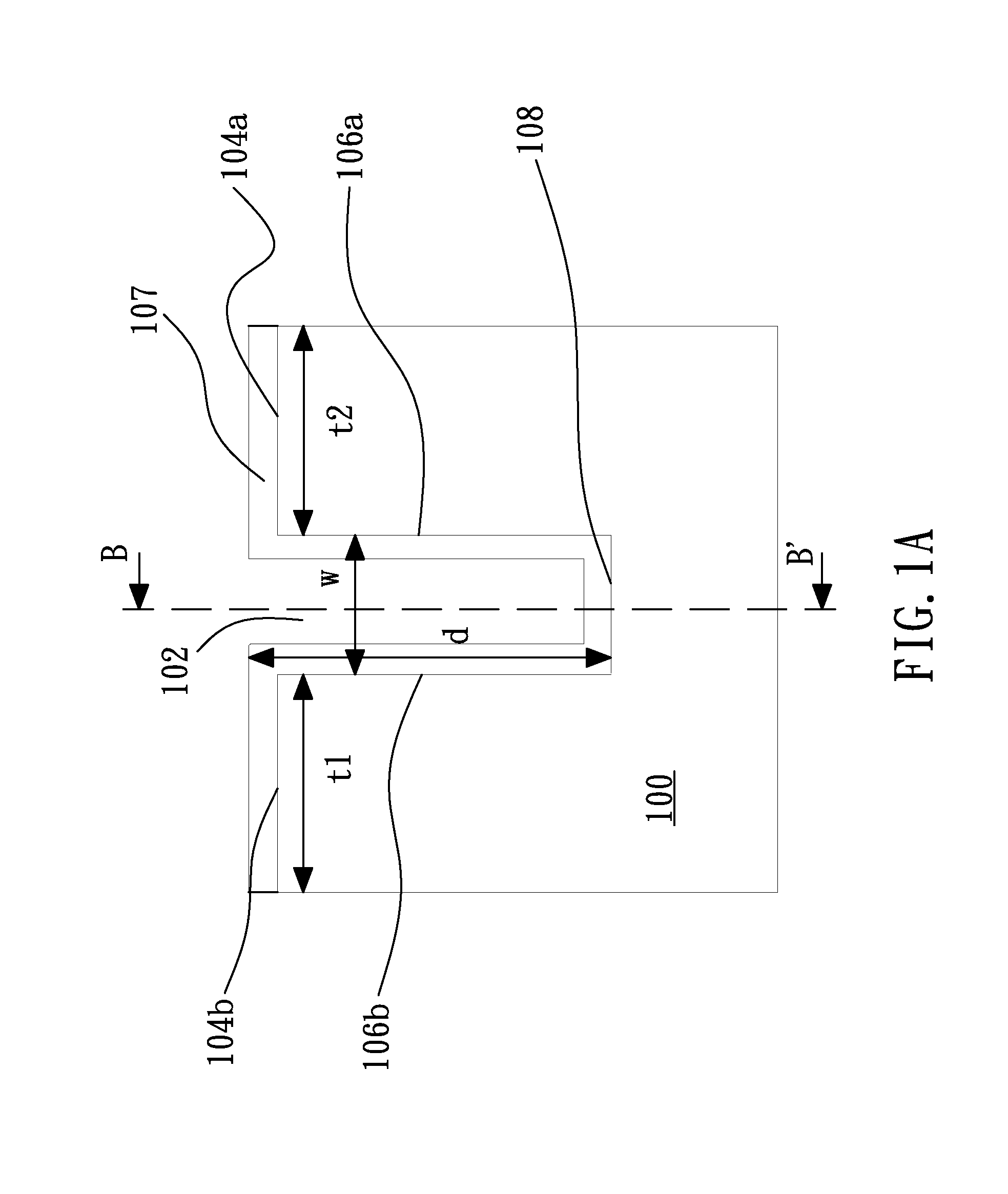
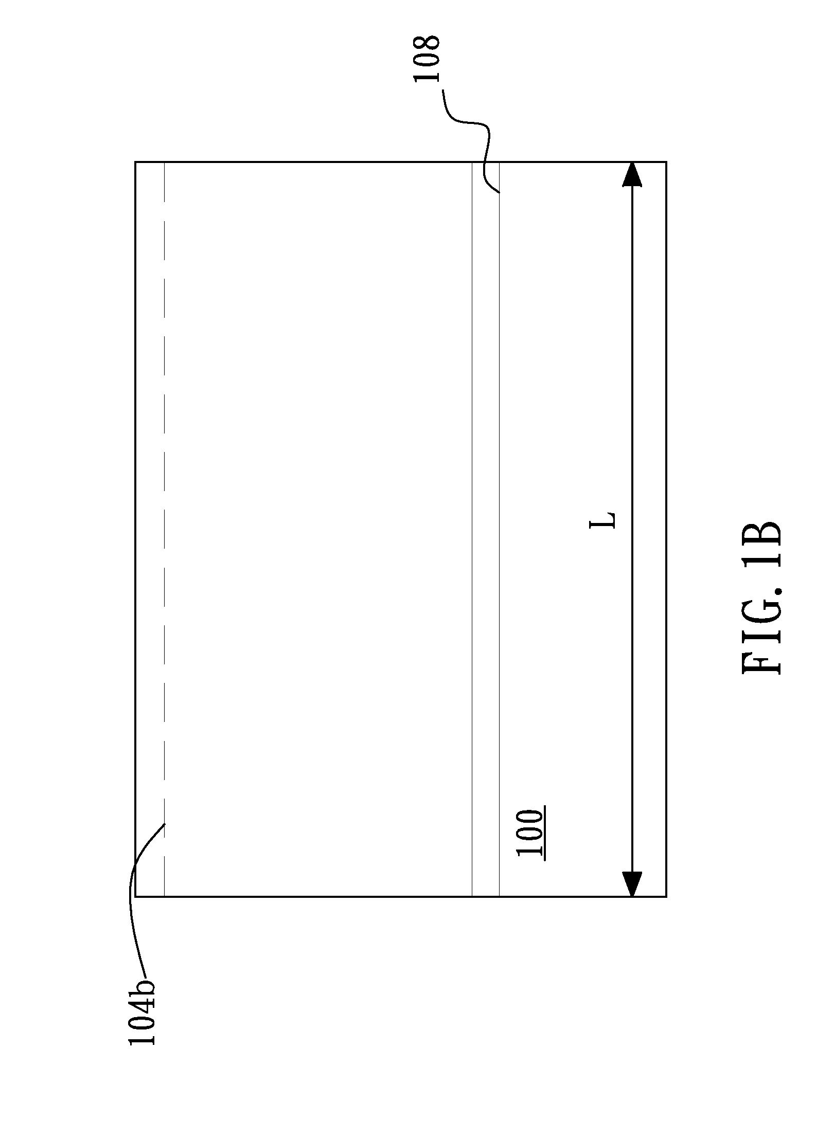
[0023]FIG. 1A illustrates a cross sectional view of a Schottky diode in accordance with one embodiment of the present invention. A trench 102 is opened in a semiconductor substrate 100 of a conductivity type, which includes a first sidewall 106a, a second sidewall 106b which is opposite to the first sidewall 106a, and a bottom mesa 108. On each side of the trench opening, there is a top mesa adjacent to the trench, for example, a first top mesa 104a is adjacent to the right-hand side of the ...


PUM


Abstract

An object of this invention is to provide a Schottky diode structure to increase the contact area at a Schottky junction between the Schottky Barrier metal and a semiconductor substrate. The larger contact area of the Schottky junction is, the lower of the forward voltage drop across the Schottky diode will be, thereby improving the performance and efficiency of the Schottky diode.
The present invention also discloses that a plurality of trenches with adjacent top mesas can be used to form a Schottky diode with even larger contact area, wherein the trenches are built using the isolation area between two cells of MOSFET with minimum extra overhead by shrinking the dimension of pitch between two trenches.

Description

FIELD OF THE INVENTION[0001]The present invention relates to a MOSFET technology and, in particular, to a MOSFET with an integrated Schottky diode.BACKGROUND OF THE INVENTION[0002]In a typical Pulse-Width-Modulation (PWM) circuit for power converters, a high side Metal Oxide Semiconductor Field-Effect Transistor (MOSFET) and a lower side MOSFET are used for rectifying purpose in order to generate an output voltage when used in a DC-DC convertor. In operating, the lower side (LS) MOSFET usually requires longer time to switch from off state to on state; and, during such time period, a body diode may turn on by a higher voltage at the drain than at the source electrode, which will cause power losses in the high side MOSFET by the current flowing from the drain electrode through the body diode to the high side MOSFET. Therefore, it is very important to prevent the body diode from turning on by using a Schottky diode in parallel with the body diode to eliminate the reverse recover loss o...

Claims


Application Information

Patent Timeline
IPC IPC(8): H01L27/06H01L21/283
CPCH01L27/0629H01L29/41766H01L29/456H01L29/47H01L29/66727H01L29/66734H01L29/872H01L29/782H01L29/0623H01L29/1095H01L29/41708H01L29/66143H01L29/7813
Inventor TAI, SUNG-SHANLI, PO-HSIENYANG, GUO-LIANGLIAO, SHIAN HAU
Owner SINOPOWER SEMICON
Why Eureka
Try Eureka