Thin-Film-Transistor Array Substrate and Manufacturing Method Thereof

a technology of thin-film transistors and array substrates, which is applied in the direction of electrical equipment, semiconductor devices, instruments, etc., can solve the problems of electrical loss and affect the operation characteristic of thin-film transistors, and achieve the effect of reducing parasitic capacitan

Active Publication Date: 2013-01-10
SHENZHEN CHINA STAR OPTOELECTRONICS TECH CO LTD
View PDF5 Cites 7 Cited by
  • Summary
  • Abstract
  • Description
  • Claims
  • Application Information

AI Technical Summary

Benefits of technology

[0009]An object of the invention is to provide a thin-film-transistor array substrate and a manufacturing method thereof to solve the problems abo...

Problems solved by technology

Besides the storage capacitor, many parasitic capacitances further exist in the actual structure of the thin-film transistor further, those parasitic ...

Method used


Image

  • Thin-Film-Transistor Array Substrate and Manufacturing Method Thereof
  • Thin-Film-Transistor Array Substrate and Manufacturing Method Thereof
  • Thin-Film-Transistor Array Substrate and Manufacturing Method Thereof

Examples


Embodiment Construction

[0044]The foregoing objects, features and advantages adopted by the present invention can be best understood by referring to the following detailed description of the preferred embodiments and the accompanying drawings. Furthermore, the directional terms described in the present invention, such as upper, lower, front, rear, left, right, inner, outer, side and etc., are only directions referring to the accompanying drawings, so that the used directional terms are used to describe and understand the present invention, but the present invention is not limited thereto.

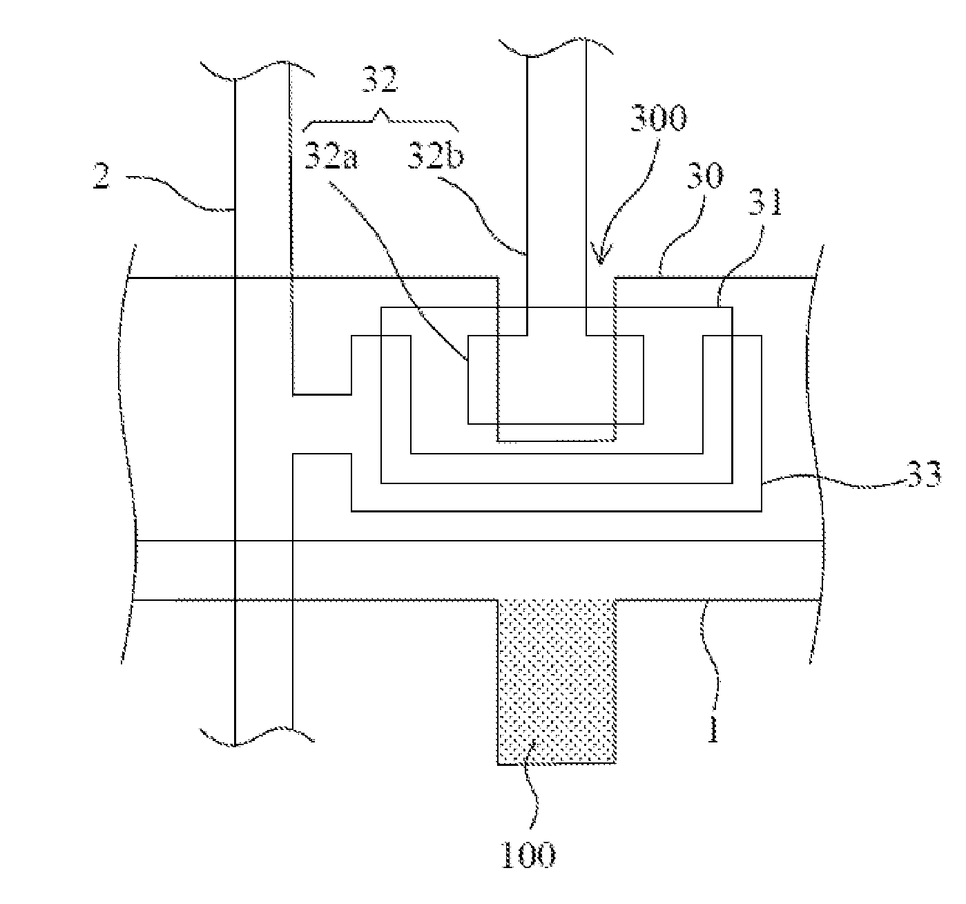
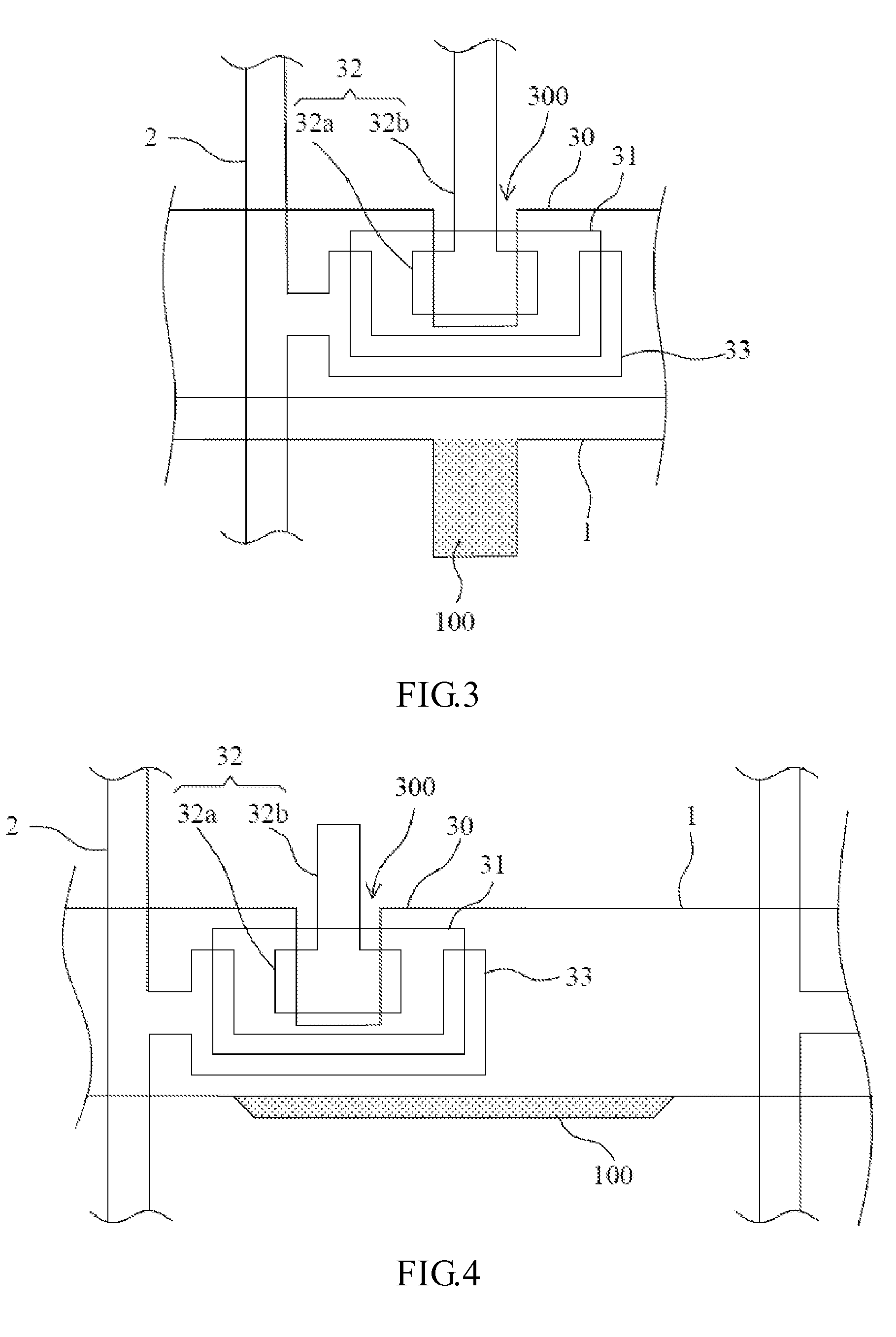
[0045]A thin-film-transistor substrate in accordance with the present invention is mainly constructed by mounting a thin-film-transistor array on a substrate. With reference to FIG. 3, FIG. 3 is a schematic diagram of a partial structure of a first embodiment of a thin-film-transistor array substrate in accordance with the present invention. As shown in FIG. 3, besides the aforementioned substrate (not shown in the figure)...


PUM


Abstract

The present invention discloses a thin-film-transistor array substrate and a manufacturing method thereof. The array substrate includes a thin-film transistor and a compensation electrode. A gate electrode of the thin-film transistor is a portion of a scan-signal line and has an opening, and the opening extends to a side of the scan-signal line. A drain electrode of the thin-film transistor is disposed correspondingly to the opening. A source electrode of the thin-film transistor extends from a side of a data-signal line and surrounds the drain electrode. The compensation electrode extends from another side of the scan-signal line and corresponds to the gate electrode. Therefore, the present invention is capable of reducing parasitic capacitance between the drain electrode and the gate electrode without increasing the resistance value of the scan-signal line.

Description

FIELD OF THE INVENTION[0001]The present invention relates to a thin-film-transistor array substrate, especially to a thin-film-transistor array substrate and a manufacturing method thereof.BACKGROUND OF THE INVENTION[0002]In conventional technologies, the structure of a TFT-LCD (Thin Film Transistor Liquid Crystal Display) mainly comprises two glass substrates and a liquid crystal layer disposed therebetween, wherein a surface of the upper glass substrate has a color filter mounted thereon, the color filter includes color filter units and black matrix; and a surface of the lower glass substrate has thin-film transistors and pixel electrodes mounted thereon, therefore it is generally called TFT Array Substrate.[0003]In a thin-film-transistor array substrate, the structure of a sub-pixel comprises a pixel electrode, a thin-film transistor and a storage capacitor, wherein a gate electrode of the thin-film transistor is connected a scan-signal line, a source electrode thereof is connect...

Claims


Application Information

Patent Timeline
IPC IPC(8): H01L27/15H01L33/08
CPCG02F1/1368H01L29/41733H01L27/124H01L29/78606H01L21/44H01L27/1259
Inventor CHANG, TSUNGLUNG
Owner SHENZHEN CHINA STAR OPTOELECTRONICS TECH CO LTD
Why Eureka
Try Eureka