Nitride semiconductor device, method for manufacturing the same and nitride semiconductor power device

a technology of nitride semiconductor and power device, which is applied in the direction of semiconductor devices, diodes, electrical devices, etc., can solve the problems of general normally-off structure degrading characteristics, current and power consumption, and limit in the efficiency of devices, so as to effectively use the normally-on hemt

Inactive Publication Date: 2013-01-10
SAMSUNG ELECTRO MECHANICS CO LTD
View PDF7 Cites 60 Cited by
  • Summary
  • Abstract
  • Description
  • Claims
  • Application Information

AI Technical Summary

Benefits of technology

[0013]An object of the present invention is to integrate a GaN power device and effectively use a normally-on HEMT.

Problems solved by technology

However, there is a limitation in the efficiency increase in devices due to a limitation of a silicon material.
Therefore, current and power are consumed.
However, a general normally-off structure may degrade characteristics, such as lowering current density and pressure resistance, or the like, in a turn-on state, as compared with the normally-on structure.
The normally-off operating device structure of FIG. 7 may use the electrical characteristics of the normally-on GaN HEMT while implementing the normally-off characteristics; however, since Vgs (gate-source voltage) of the normally-on GaN HEMT is a negative value approximating 0V when being turned-on, the normally-off operating device prevents a large amount of Ids (drain-source current) from flowing, thereby increasing the turn-on resistance and increasing the switching loss of the device.

Method used


Image

  • Nitride semiconductor device, method for manufacturing the same and nitride semiconductor power device
  • Nitride semiconductor device, method for manufacturing the same and nitride semiconductor power device
  • Nitride semiconductor device, method for manufacturing the same and nitride semiconductor power device

Examples


Embodiment Construction

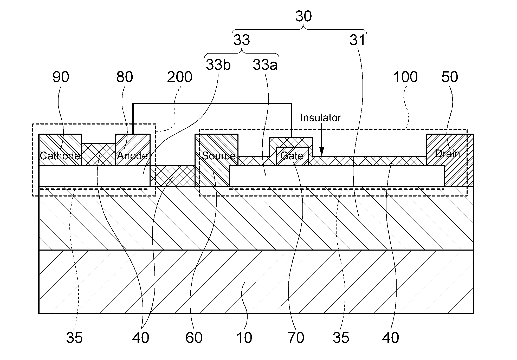
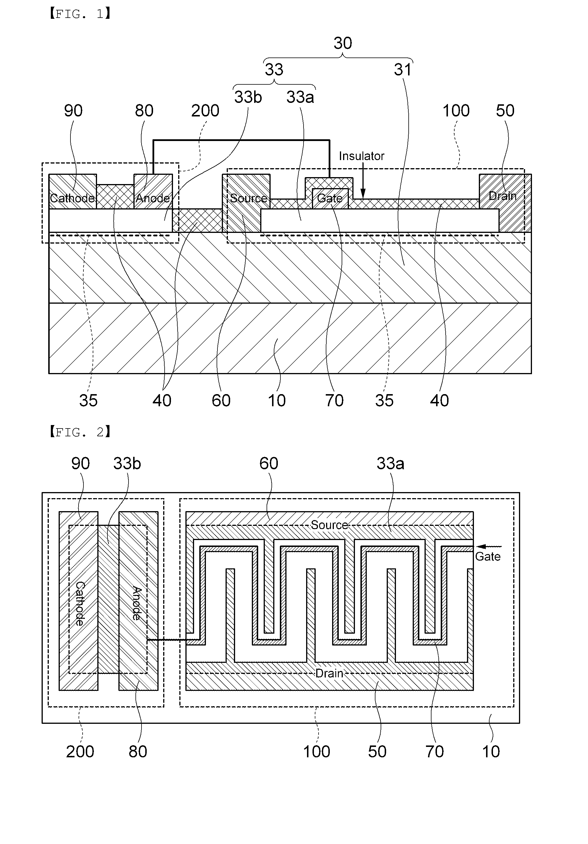
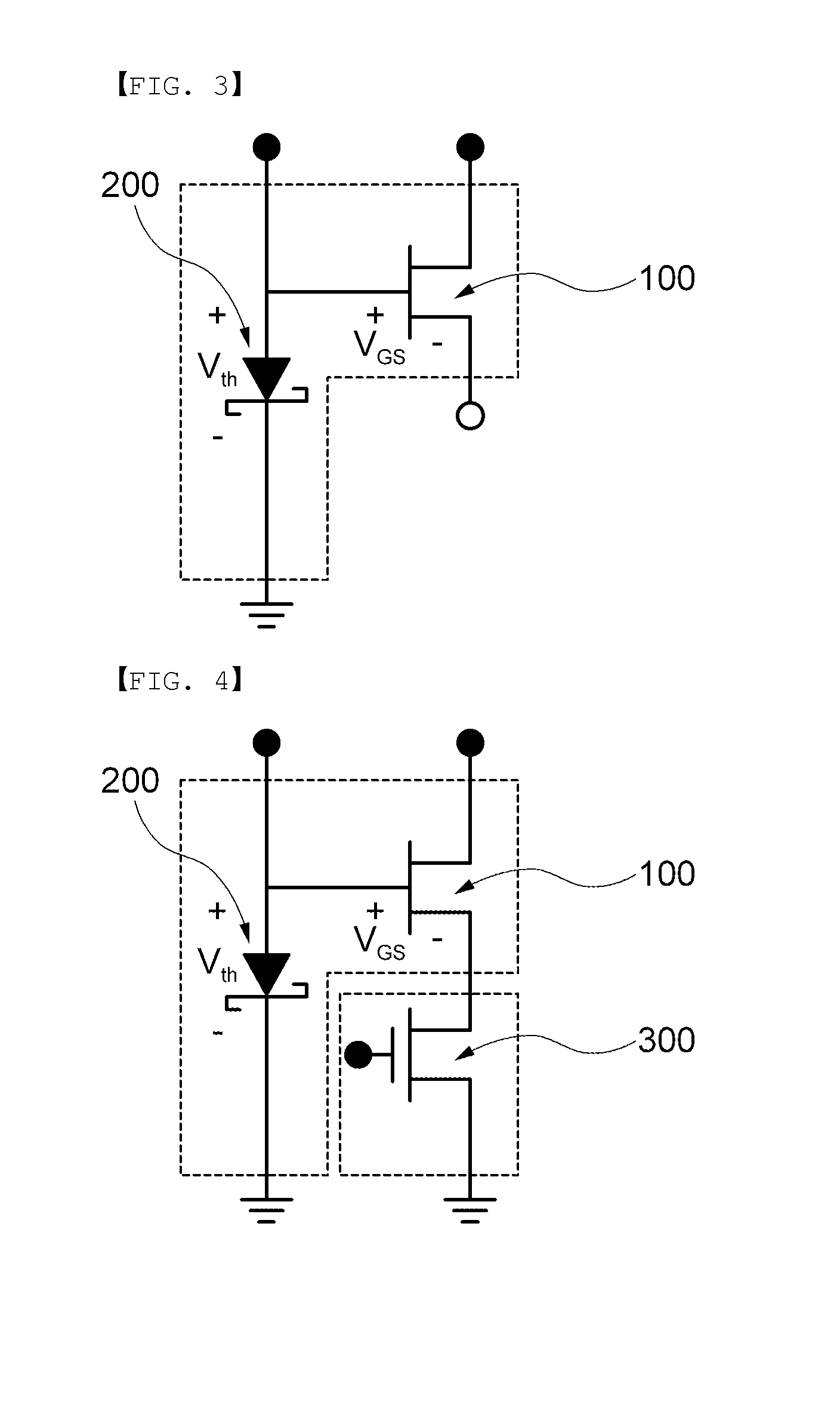
[0042]Exemplary embodiments of the present invention for accomplishing the above-mentioned objects will be described with reference to the accompanying drawings. In describing exemplary embodiments of the present invention, the same reference numerals will be used to describe the same components and an additional description that is overlapped or allow the meaning of the present invention to be restrictively interpreted will be omitted.

[0043]It will be understood that when an element is simply referred to as being ‘connected to’ or ‘coupled to’ another element without being ‘directly connected to’ or ‘directly coupled to’ another element in the present description, it may be ‘directly connected to’ or ‘directly coupled to’ another element or be connected to or coupled to another element, having the other element intervening therebetween. In addition, in the specification, spatially relative terms, ‘on’, ‘above’, ‘upper’, ‘below’, ‘lower’, or the like, they should be interpreted as b...


PUM

PropertyMeasurementUnit
gate voltageaaaaaaaaaa
gate driving voltageaaaaaaaaaa
semiconductoraaaaaaaaaa

Abstract

Disclosed herein are a nitride semiconductor device, a method for manufacturing the same, and a nitride semiconductor power device. According to an exemplary embodiment of the present invention, a nitride semiconductor device includes: a nitride semiconductor layer over a substrate wherein the nitride semiconductor layer has a two-dimensional electron gas (2DEG) channel formed therein; a D-mode FET that includes a gate electrode Schottky-contacting with the nitride semiconductor layer to form a normally-on operating depletion-mode (D-mode) HEMT structure; and a Schottky diode part that includes an anode electrode Schottky-contacting with the nitride semiconductor layer and increases a gate driving voltage of the D-mode FET, the anode electrode being connected to the gate electrode of the D-mode FET. In addition, the nitride semiconductor power device and the method for manufacturing a nitride semiconductor device are proposed.

Description

[0001]CROSS REFERENCE(S) TO RELATED APPLICATIONS[0002]This application claims the benefit under 35 U.S.C. Section 119 of Korean Patent Application Serial No. 10-2011-0065922, entitled “Nitride Semiconductor Device, Method For Manufacturing The Same And Nitride Semiconductor Power Device” filed on Jul. 4, 2011, which is hereby incorporated by reference in its entirety into this application.BACKGROUND OF THE INVENTION[0003]1. Technical Field[0004]The present invention relates to a nitride semiconductor device, a method for manufacturing the same, and a nitride semiconductor power device. More particularly, the present invention relates to a nitride semiconductor device for effectively using integration of a GaN power device and a normally-on HEMT, a method for manufacturing the same, and a nitride semiconductor power device.[0005]2. Description of the Related Art[0006]A focus on saving power consumption has been increased due to a green energy policy, or the like. To this end, there i...

Claims


Application Information

Patent Timeline
Patent Type & Authority Applications(United States)
IPC IPC(8): H01L29/778H01L21/335H01L27/06
CPCH01L21/8252H01L29/66462H01L29/7787H01L27/0605H01L29/2003H01L27/0883H01L29/872H01L29/0692H01L27/0629H01L21/18H01L29/778
Inventor PARK, YOUNG HWANPARK, KI YEOLJEON, WOO CHUL
Owner SAMSUNG ELECTRO MECHANICS CO LTD
Why Eureka
Try Eureka