Liquid crystal display device and method for producing same
a technology of liquid crystal display and liquid crystal, which is applied in the direction of optics, coatings, instruments, etc., can solve the problems of low power consumption, reduced luminance, thin and lightweight liquid crystal display devices, etc., and achieves favorable alignment conditions, reduce and reduce the effect of vhr and image sticking
- Summary
- Abstract
- Description
- Claims
- Application Information
AI Technical Summary
Benefits of technology
Problems solved by technology
Method used
Image
Examples
first embodiment
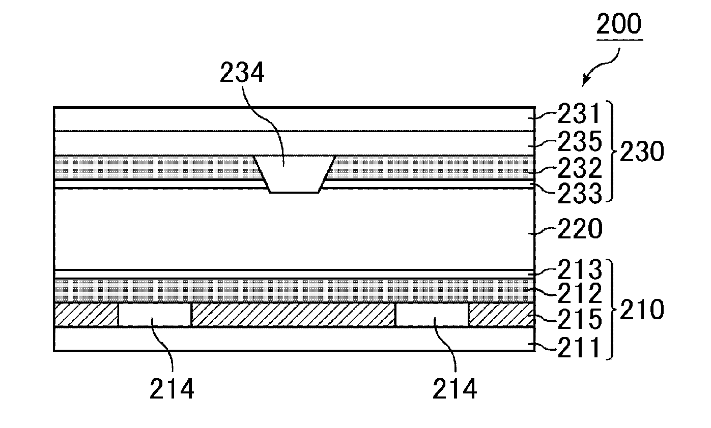
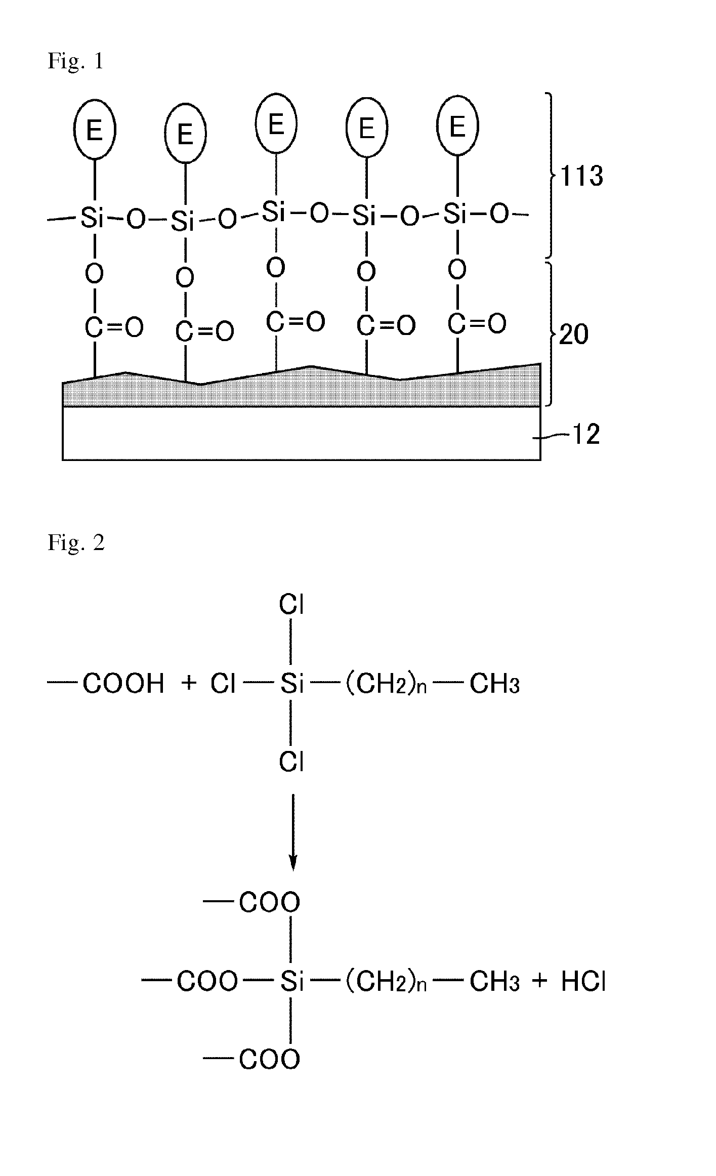
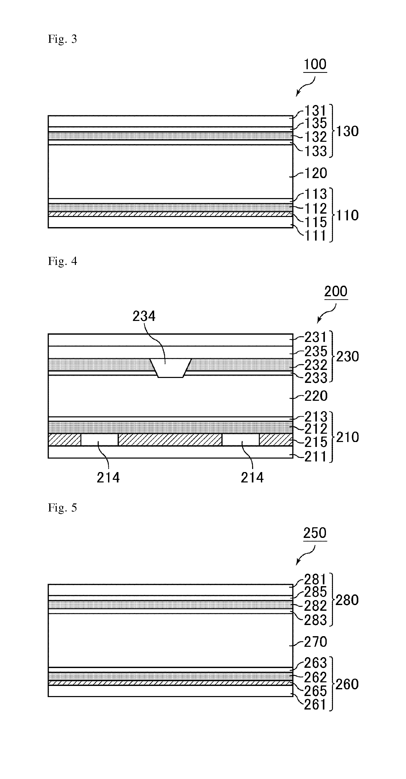
[0110]In the present embodiment, description will be made with an example of a TN-mode liquid crystal display device having horizontal alignment films that horizontally align liquid crystals. FIG. 3 is a schematic cross-sectional view illustrating the structure of the liquid crystal display device of the present embodiment.
[0111]In FIG. 3, a liquid crystal display device 100 is provided with a TFT array substrate 110, a counter substrate 130 disposed to face the TFT array substrate 110, and a liquid crystal layer 120 disposed between the TFT array substrate 110 and the counter substrate 130.
[0112]The TFT array substrate 110 has, on the liquid crystal layer 120-side main surface of a glass substrate (supporting substrate 111), multiple gate signal lines parallel to each other, multiple source signal lines perpendicular to the gate signal lines and extending in parallel to each other, and thin film transistors (TFTs) disposed at each crossing portion of a gate signal line and a source...
examples 1 to 5
[0127]In the same manner as in the first embodiment, TN-mode liquid crystal display devices of Examples 1 to 5 were produced which included monomolecular films formed using chlorosilane-based surfactants having different linear alkyl chain lengths. Specifically, in Example 1, monomolecular films were formed using a chlorosilane-based surfactant with n in the above chemical formula=3. Similarly, monomolecular films were formed using chlorosilane-based surfactants with n=5 in Example 2, n=7 in Example 3, n=9 in Example 4, and n=11 in Example 5.
[0128]The pretilt angle, VHR, and residual DC voltage of each of the liquid crystal display devices were measured. The obtained results are shown in Table 1.
second embodiment
[0134]Monomolecular films were formed using a chlorosilane-based surfactant represented by the chemical formula Cl3Si—(CH2)n—NH2 instead of a chlorosilane-based surfactant represented by the chemical formula Cl3Si—(CH2)n—CH3. Except for that, a TN-mode liquid crystal display device having horizontal alignment films was produced in the same manner as in the first embodiment.
[0135]Hereinafter, the present embodiment will be described in more detail based on examples and comparative examples.
PUM
| Property | Measurement | Unit |
|---|---|---|
| pretilt angle | aaaaa | aaaaa |
| pretilt angle | aaaaa | aaaaa |
| pretilt angle | aaaaa | aaaaa |
Abstract
Description
Claims
Application Information


