Column a/d converter, column a/d conversion method, solid-state imaging element and camera system

a conversion method and converter technology, applied in the field of columns a/d converters, column a/d conversion methods, solid-state imaging elements and camera systems, can solve the problems of reducing clock duty, reducing clock duty, and increasing the power consumed by the counter of each column

Active Publication Date: 2013-01-17
SONY CORP
View PDF3 Cites 26 Cited by
  • Summary
  • Abstract
  • Description
  • Claims
  • Application Information

AI Technical Summary

Benefits of technology

[0033]An example of a solid-state imaging device includes a column processing section that includes a low-level bit latching section. The low-level bit latching section receives a comparator output from a comparator and a count output from a counter, and the low-level bit latching section latches a count value.
[0034]Another example of a solid-state imaging device includes a counter and a plurality of column processing sections. Each of the column processing sections includes a comparator and a low-level bit latching section. And within each of the column processing section, the low-level bit latching section receives a comparator output from the comparator and a count output from the counter, and the low-level bit latching section latches a count value.
[0035]An example of an analog-digital conversion method includes outputting a comparator output to a low-level bit latching section, outputting a count output to the low-level bit latching section, and latching a count value with the low-level bit latching section.
[0036]Another example of an analog-digital conversion method includes outputting comparator outputs to a plurality of low-level bit latching sections, outputting a count output to the low-level bit latching sections, and latching count values with the low-level bit latching sections.

Problems solved by technology

As a result, if clock frequency increases and the number of horizontal columns becomes large, power consumed by the counter of each column increases, and if the product characteristics deteriorate, there are adverse effects such as a fall in operation margins due to IR drop and the like at the same time.
Additionally, due to a large burden on a standard clock line, degrading of clock duty becomes larger as the standard clock becomes faster and there is a limit on AD resolution.

Method used


Image

  • Column a/d converter, column a/d conversion method, solid-state imaging element and camera system
  • Column a/d converter, column a/d conversion method, solid-state imaging element and camera system
  • Column a/d converter, column a/d conversion method, solid-state imaging element and camera system

Examples


Embodiment Construction

[0060]Below, embodiments of the invention will be associated with the drawings and described.

[0061]1. Example of Overall Configuration of Solid-State Imaging Element

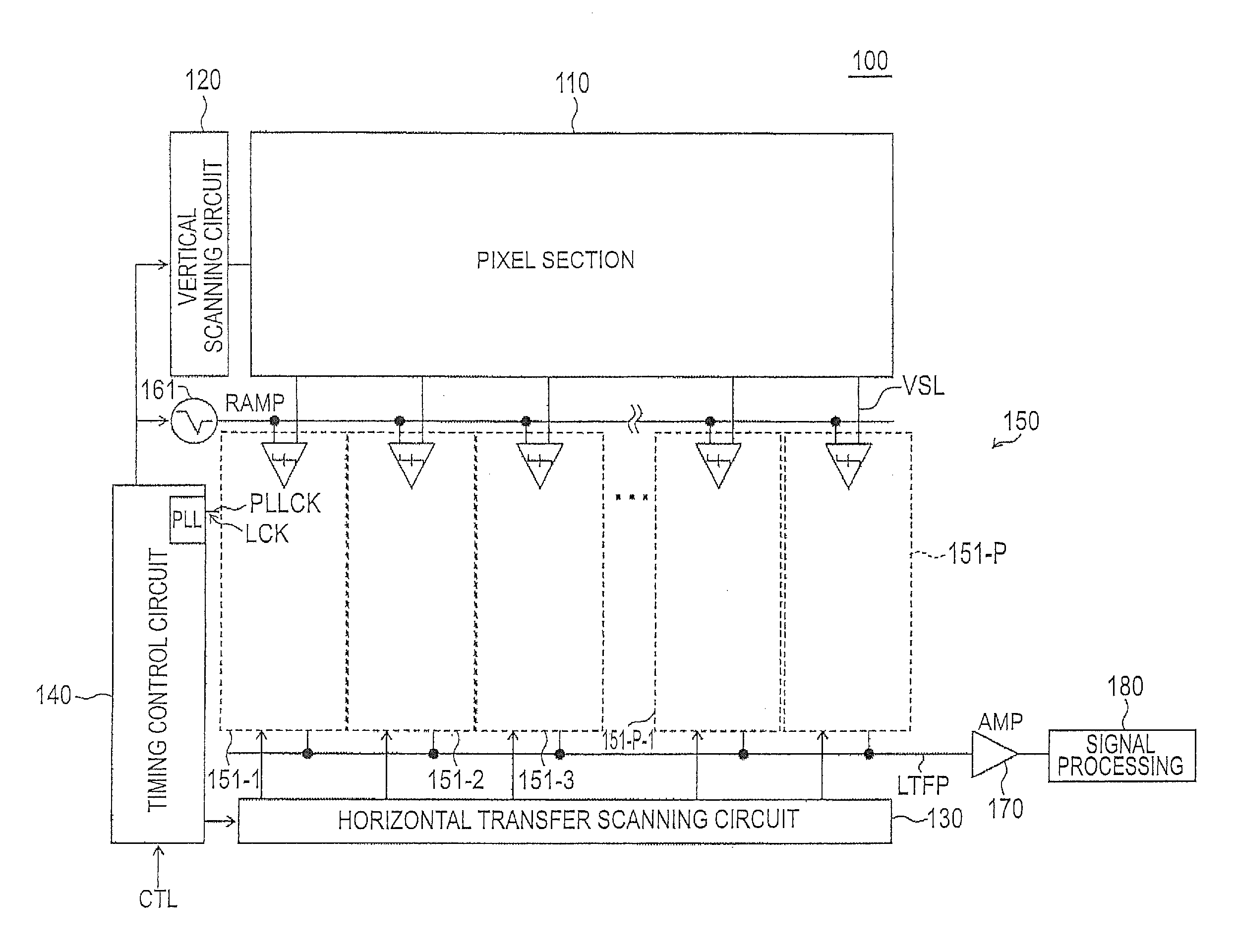
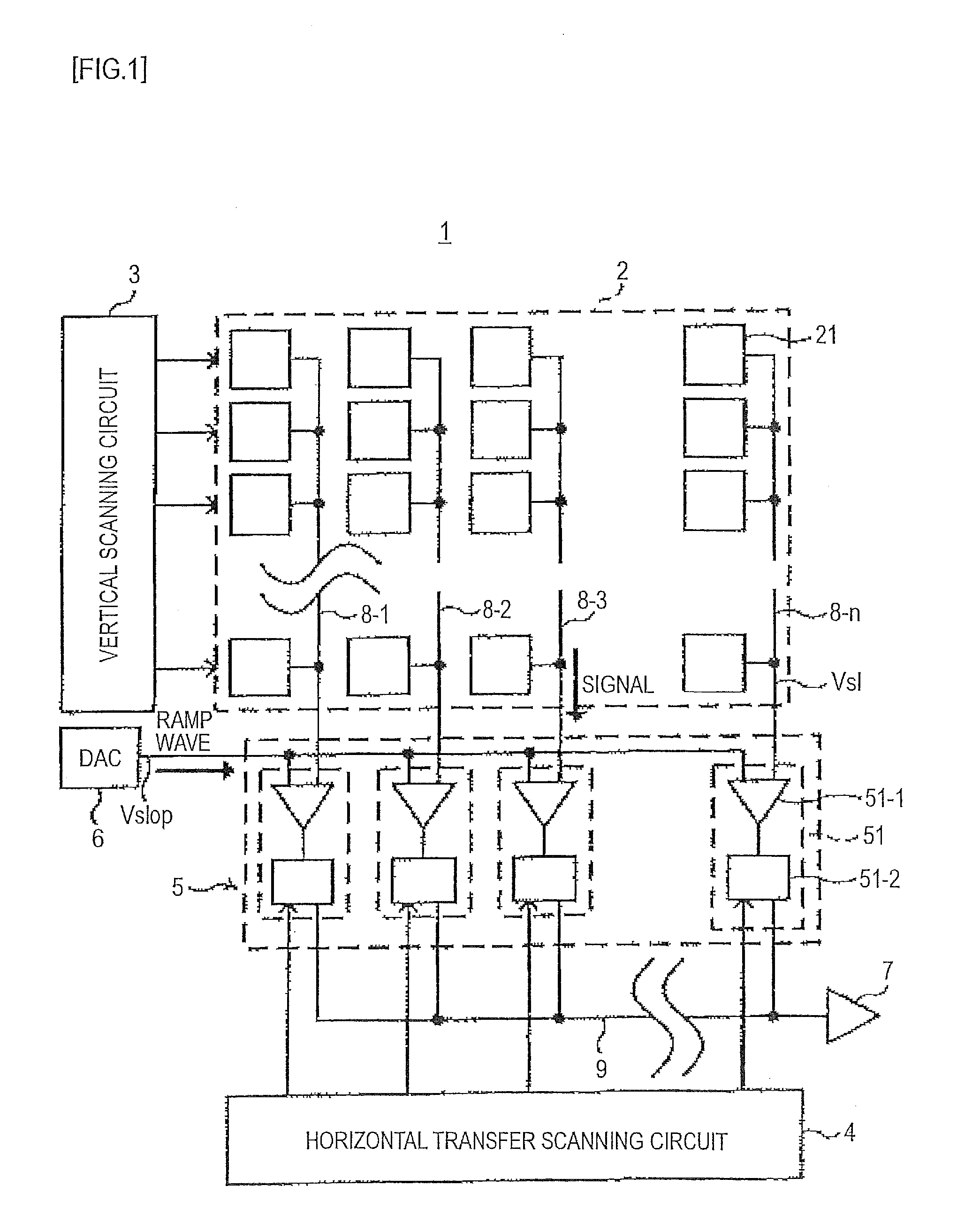
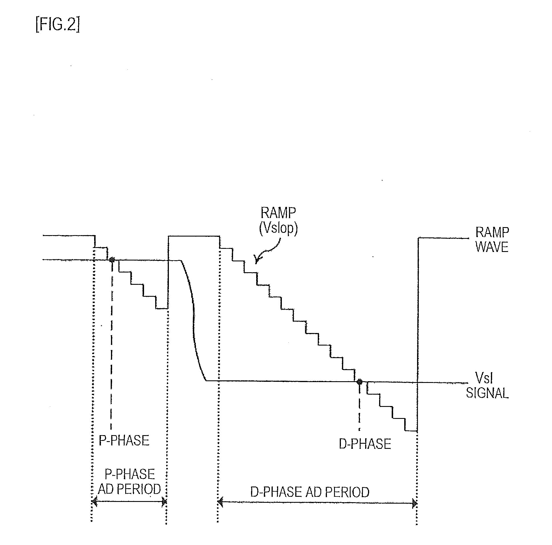
[0062]FIG. 3 is a block diagram illustrating a configuration example of a solid-state imaging element mounted with a column parallel ADC (CMOS image sensor) according to an embodiment of the invention.

[0063]FIG. 4 is a block diagram illustrating in more detail the main sections of the solid-state imaging element mounted with a column parallel ADC (CMOS image sensor) shown in FIG. 3.

[0064]As shown in FIGS. 3 and 4, a solid-state imaging element 100 has a pixel section 110 which is an imaging section, a vertical scanning circuit 120, a horizontal transfer scanning circuit 130, a timing control circuit 140, and a column A / D converter (ADC) 150 which is a pixel signal read out section. In addition, the pixel signal read out section is configured including the vertical scanning circuit 120 and the like.

[0065]The solid-state i...


PUM


Abstract

A solid-state imaging device having an analog-digital converter, and an analog-digital conversion method are described herein. An example of a solid-state imaging device includes a column processing section that includes a low-level bit latching section. The low-level bit latching section receives a comparator output from a comparator and a count output from a counter, and the low-level bit latching section latches a count value.

Description

TECHNICAL FIELD[0001]The invention relates to a column A / D converter which is able be applied to a solid-state imaging element or the like of a CMOS image sensor or the like, a column A / D conversion method, a solid-state imaging element, and a camera system.BACKGROUND ART[0002]A CMOS image sensor is proposed which has a pixel array section provided as a plurality of pixels in a two dimensional alignment, sequentially reads out a pixel signal read from each pixel of the pixel array section for each of the pixel columns, performs CDS processing and the like on each column signal, and converts and outputs the image signals.[0003]A column parallel output type of the CMOS image sensor, which has an FD amplifier having a floating diffusion (FD) layer for each pixel and in which the output thereof is performed by selecting one row from among the pixel arrays and reading out the selected row simultaneously in the column direction, is predominant.[0004]This is because parallel processing is ...

Claims


Application Information

Patent Timeline
Patent Type & Authority Applications(United States)
IPC IPC(8): H03M1/12H01L27/146H03M1/34
CPCH04N5/3765H03M1/56H03M1/0872H04N5/378H04N25/745H04N25/75H03M1/002H03M1/36H03M7/16
Inventor IWAKI, HIROYUKI
Owner SONY CORP
Why Eureka
Try Eureka