Method of manufacturing a mask blank substrate, method of manufacturing a mask blank, method of manufacturing a transfer mask, and method of manufacturing a semiconductor device

a technology of transfer mask and mask blank, which is applied in the direction of photomechanical equipment, originals for photomechanical treatment, instruments, etc., can solve the problems of difficult to satisfy demand, degraded transfer accuracy, and increased demand for further miniaturization, so as to ensure the approximation accuracy, facilitate and accurately perform the calculation of position shift, the effect of shortening the calculation tim

Active Publication Date: 2013-01-24
HOYA CORP
View PDF0 Cites 7 Cited by
  • Summary
  • Abstract
  • Description
  • Claims
  • Application Information

AI Technical Summary

Benefits of technology

[0047]In this invention, simulation results are not used as they are, but data of an approximate curved surface is used for correcting a transfer pattern and, in the approximate curved surface, data are interpolated for regions (gaps) between measurement points where height information of a substrate main surface is obtained. Therefore, it is possible to easily and accurately perform calculation of position shift amounts and correction of a design transfer pattern also for the regions between the measurement points. Further, since a polynomial curved surface of about the fourth to sixth order is selected as an approximate curved surface, it is possible to shorten the calculation time and simultaneously to ensure the approximation accuracy.

Problems solved by technology

However, a demand for further miniaturization has been increasing and such a demand is difficult to satisfy only by using the ArF excimer laser light as the exposure light source.
Thus, the transfer accuracy has been degraded.
However, there has been a problem that, although the shape of a main surface of the substrate can be estimated somewhat accurately by the simulation of the substrate shape using the finite element method, the simulation is very time-consuming.

Method used


Image

  • Method of manufacturing a mask blank substrate, method of manufacturing a mask blank, method of manufacturing a transfer mask, and method of manufacturing a semiconductor device
  • Method of manufacturing a mask blank substrate, method of manufacturing a mask blank, method of manufacturing a transfer mask, and method of manufacturing a semiconductor device
  • Method of manufacturing a mask blank substrate, method of manufacturing a mask blank, method of manufacturing a transfer mask, and method of manufacturing a semiconductor device

Examples


example

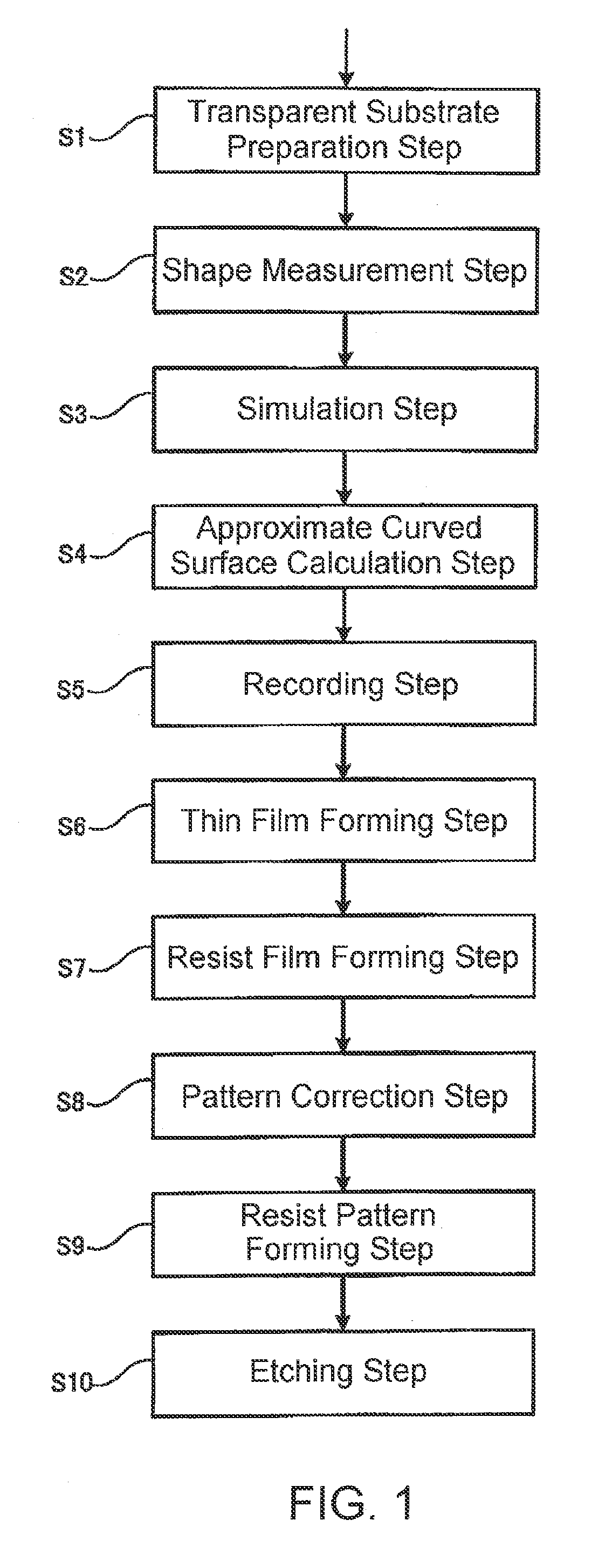
[0119]Hereinbelow, exposure mask manufacturing steps including mask blank transparent substrate manufacturing steps and mask blank manufacturing steps will be described in detail.

[0120](I) Transparent Substrate Preparation Step (S1)

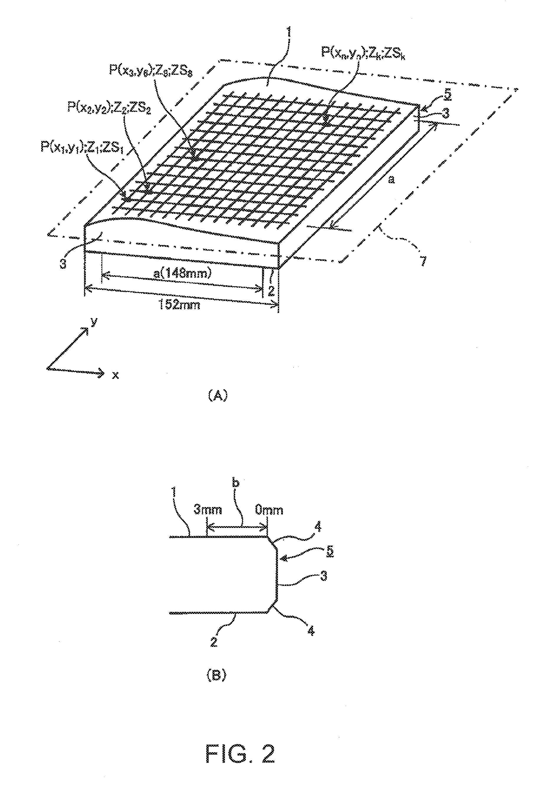
[0121]Main surfaces of square transparent substrates (synthetic quartz glass substrates) were precision-polished and cleaned, thereby preparing two transparent substrates (about 152 mm×about 152 mm×6.35 mm). In this event, using a carbon dioxide laser, a data matrix with a block size of 3 mm×3 mm was formed as an identification mark on an end face of each transparent substrate. In the data matrix, the symbol size was set to 12×12 (fixed: 10 digits) and the cell size was set to 0.25 mm. With this identification mark, a 10-digit serial number was assigned to each transparent substrate.

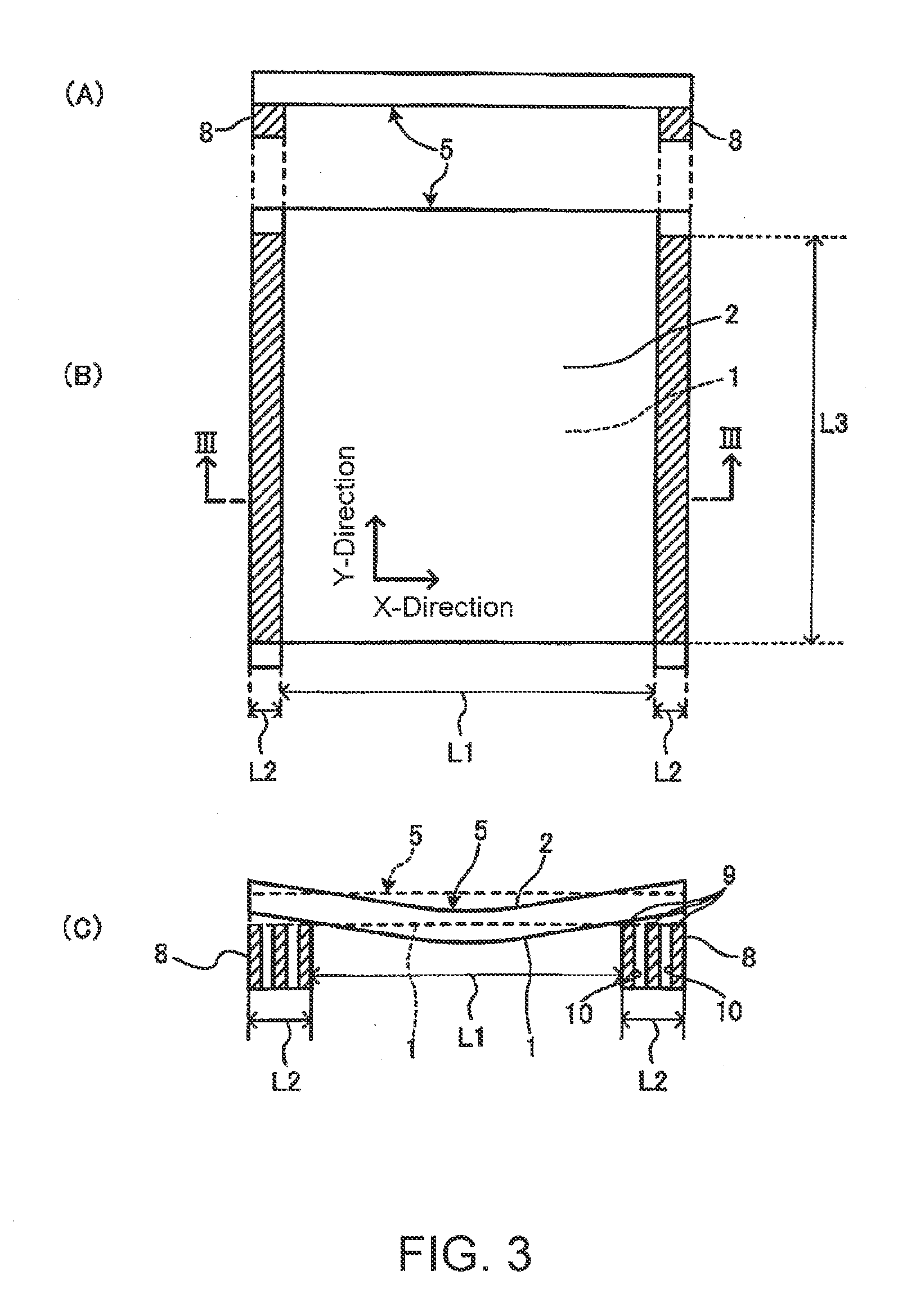
[0122](II) Shape Measurement Step (S2)

[0123]With respect to each transparent substrate, using a flatness measuring apparatus (UltraFlat200M manufactured by Corning TROPEL Corp...


PUM

PropertyMeasurementUnit
flatnessaaaaaaaaaa
flatnessaaaaaaaaaa
wavelengthaaaaaaaaaa

Abstract

In a simulation step of simulating a surface configuration of a substrate which is used for a mask blank and which is set to an exposure apparatus, height information from a reference plane is derived from a plurality of measurement points on a main surface of the substrate. From the height information, a curved surface of fourth, fifth, or sixth order is approximated which is represented by a polynomial specified by a plurality of terms and coefficients of the terms. The coefficients are stored as coefficient information in association with the substrate.

Description

TECHNICAL FIELD[0001]This invention relates to a method of manufacturing a mask blank substrate, a method of manufacturing a mask blank, a method of manufacturing a transfer mask, and a method of manufacturing a semiconductor device in the semiconductor field.BACKGROUND ART[0002]With the miniaturization of semiconductor devices in recent years, the reduction in the wavelength of an exposure light source for use in the photolithography technique has been proceeding. In the advanced transmission photolithography field, an ArF excimer laser (wavelength 193 nm) with a wavelength of 200 nm or less is used as an exposure light source. However, a demand for further miniaturization has been increasing and such a demand is difficult to satisfy only by using the ArF excimer laser light as the exposure light source. In order to satisfy the demand, an increase of NA (numerical number) has been adopted by using the oblique illumination method or the like. With the increase in NA, however, the fo...

Claims


Application Information

Patent Timeline
Patent Type & Authority Applications(United States)
IPC IPC(8): G06F17/50G03F1/50G03F7/20
CPCG03F1/50G03F1/70
Inventor TANABE, MASARU
Owner HOYA CORP
Why Eureka
Try Eureka