Method for manufacturing ferroelectric device

a manufacturing method and technology for ferroelectric devices, applied in the direction of device material selection, optical radiation measurement, instruments, etc., can solve the problems of increasing manufacturing costs, and achieve the effects of reducing costs, simplifying manufacturing processes, and improving crystallinity and performance of ferroelectric films

Inactive Publication Date: 2013-01-24
PANASONIC CORP
View PDF13 Cites 16 Cited by
  • Summary
  • Abstract
  • Description
  • Claims
  • Application Information

AI Technical Summary

Benefits of technology

[0032]With the method for manufacturing a ferroelectric device according to the present invention, crystallinity and performance of a

Problems solved by technology

As a result, manufact

Method used


Image

  • Method for manufacturing ferroelectric device
  • Method for manufacturing ferroelectric device
  • Method for manufacturing ferroelectric device

Examples


first embodiment

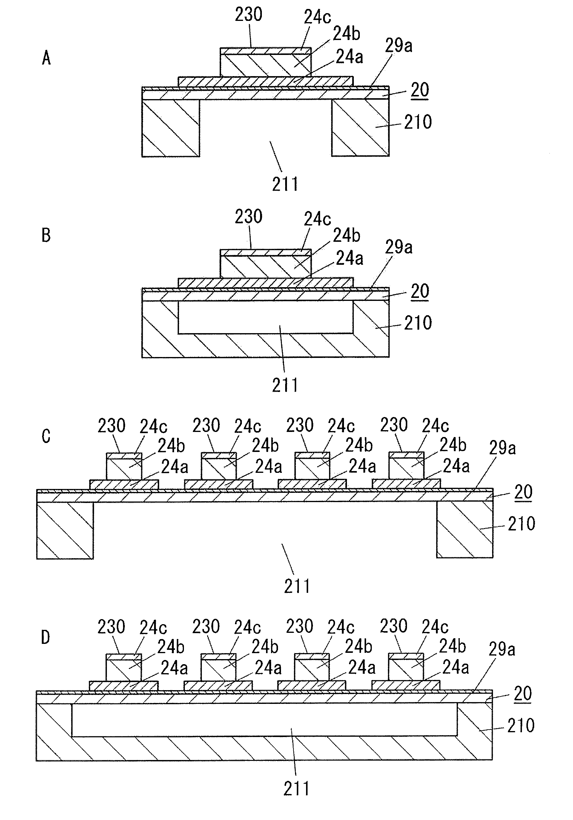
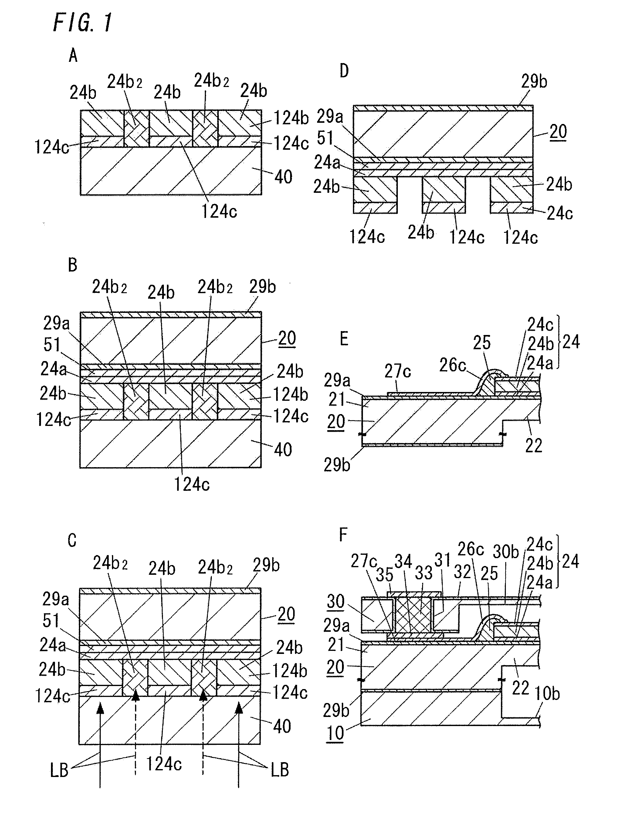
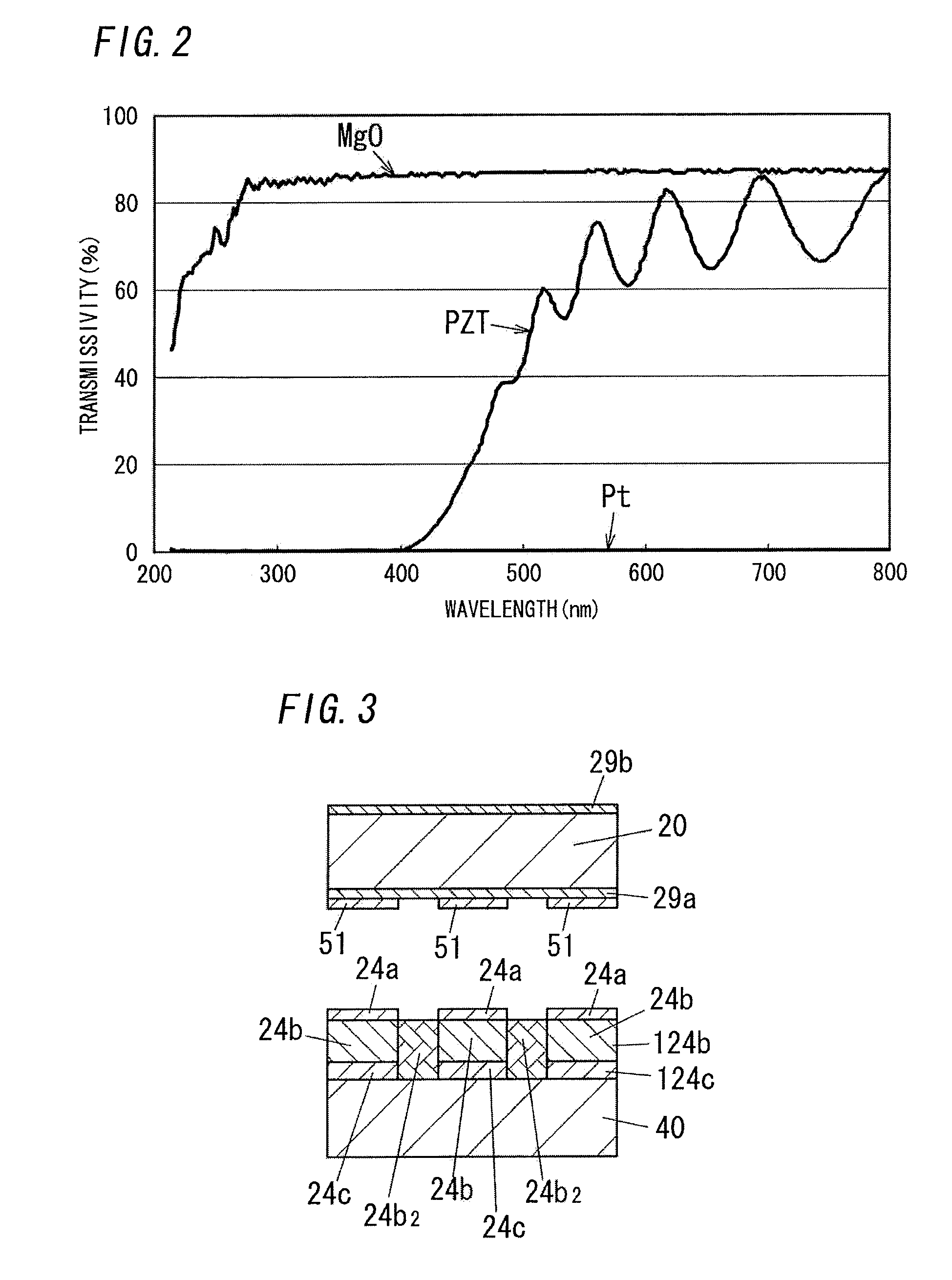
[0042]First, a ferroelectric device according to the present embodiment will be described with reference to FIGS. 4 to 6 and, subsequently, a manufacturing method will be described with reference to FIGS. 1 to 3.

[0043]A ferroelectric device comprises a lower electrode 24a formed on one surface of a first substrate 20, a ferroelectric film 24b formed on an opposite side of the lower electrode 24a to the first substrate 20, and an upper electrode 24c formed on an opposite side of the ferroelectric film 24b to the lower electrode 24a. In this case, the ferroelectric film 24b is formed of a ferroelectric material having difference in lattice constants from the first substrate 20.

[0044]Moreover, one surface of the first substrate in a thickness direction of the first substrate is defined as a first surface of the first substrate, and the side of other surface of the first substrate in the thickness direction of the first substrate is defined as a second surface of the first substrate.

[00...

second embodiment

[0095]First, a ferroelectric device according to the present embodiment will be described with reference to FIG. 8F and, subsequently, a manufacturing method will be described with reference to FIG. 8.

[0096]As shown in FIG. 8F, a ferroelectric device according to the present embodiment comprises a lower electrode 24a formed on aside of one surface (a first surface side) of a first substrate 20, a ferroelectric film 24b formed on an opposite side of the lower electrode 24a to the first substrate 20, and an upper electrode 24c formed on an opposite side of the ferroelectric film 24b to the side of the lower electrode 24a. In this case, the ferroelectric film 24b is formed of a ferroelectric material that has difference in lattice constants from the first substrate 20. Moreover, components of the ferroelectric device that are similar to those in the first embodiment are denoted by the same reference characters.

[0097]The ferroelectric device according to the present embodiment is a pyro...


PUM

PropertyMeasurementUnit
Wavelengthaaaaaaaaaa
Temperatureaaaaaaaaaa
Lattice constantaaaaaaaaaa

Abstract

A seed layer having a predetermined pattern is formed on a side of one surface of a second substrate, and a ferroelectric layer is formed on the side of the one surface of the second substrate. A lower electrode is formed on the ferroelectric layer, and the lower electrode and a first substrate are bonded via a bonding layer. A laser beam with a predetermined wavelength is irradiated from a side of other surface of the second substrate to transfer a ferroelectric film, which overlaps with the seed layer, of the ferroelectric layer and the seed layer onto the side of said one surface of the first substrate. The laser beam passes through the second substrate, is reflected by the seed layer, and is absorbed by a second portion of the ferroelectric layer. The second portion does not overlap with the seed layer.

Description

TECHNICAL FIELD[0001]The present invention relates to a method for manufacturing a ferroelectric device that uses a piezoelectric effect or a pyroelectric effect of a ferroelectric film.BACKGROUND ART[0002]Conventionally, ferroelectric devices that use a piezoelectric effect or a pyroelectric effect of a ferroelectric film have been attracting attention.[0003]As an example of a ferroelectric device of this type, conventionally, a MEMS (micro electro mechanical systems) device comprising a ferroelectric film as a function membrane has been proposed. As MEMS devices of this type, for example, a power-generating device and an actuator which use a piezoelectric effect of a ferroelectric film, and pyroelectric devices such as a pyroelectric infrared sensor which use a pyroelectric effect of a ferroelectric film are being developed at various facilities. Moreover, as a ferroelectric material that exhibits both a piezoelectric effect and a pyroelectric effect, for example, PZT (:Pb(Zr,Ti)O...

Claims


Application Information

Patent Timeline
IPC IPC(8): H01L21/30B81C3/00H01L21/8246G01J1/02H01L27/105H01L41/08H01L41/113H01L41/18H01L41/22H01L41/313H01L41/316H01L41/319H01L41/33H01L41/39
CPCG01J5/34H01L28/56H01L41/319H01L41/1136H01L41/313H01L37/02H10N15/10H10N30/306H10N30/073H10N30/079G01J1/02H10N30/30H10N30/01
Inventor MATSUSHIMA, TOMOAKIYAMAUCHI, NORIHIROOGAWA, JUNYAAIZAWA, KOICHI
Owner PANASONIC CORP
Why Eureka
Try Eureka