Display device and method of fabricating the same

a technology of a display device and a fabrication method, which is applied in the direction of paper/cardboard containers, electrical apparatus casings/cabinets/drawers, instruments, etc., can solve the problems of tape having a working limit of about 1.0 mm, tape cannot be designed to have a narrow bezel of a width smaller than about 1.0 mm, and the fabrication cost is reduced, so as to prevent light leakage through a side surface.

Active Publication Date: 2013-01-31
LG DISPLAY CO LTD
View PDF5 Cites 75 Cited by
  • Summary
  • Abstract
  • Description
  • Claims
  • Application Information

AI Technical Summary

Benefits of technology

[0019]Another object of the present invention is to provide a display device where a light leakage through a side surface is prevented due to an adhesive and a method of fabricating the display device.
[0020]Another object of the present invention is to provide a display device where a fabrication cost is reduced due to an adhesive and a method of fabricating the display device.

Problems solved by technology

However, since the tape has a working limit of about 1.0 mm, the LCD device using the tape for the liquid crystal panel can not have a narrow bezel of a width smaller than about 1.0 mm.
For example, the tape can not be designed to have a width smaller than about 1.0 mm due to the working limit.
As a result, it is difficult to obtain the LCD device having a narrow bezel.
However, another part of light from the backlight unit may penetrate the main frame of a white colored material to generate a light leakage through a side surface of the LCD device.
As a result, fabrication cost of the LCD device increases.

Method used


Image

  • Display device and method of fabricating the same
  • Display device and method of fabricating the same
  • Display device and method of fabricating the same

Examples


first embodiment

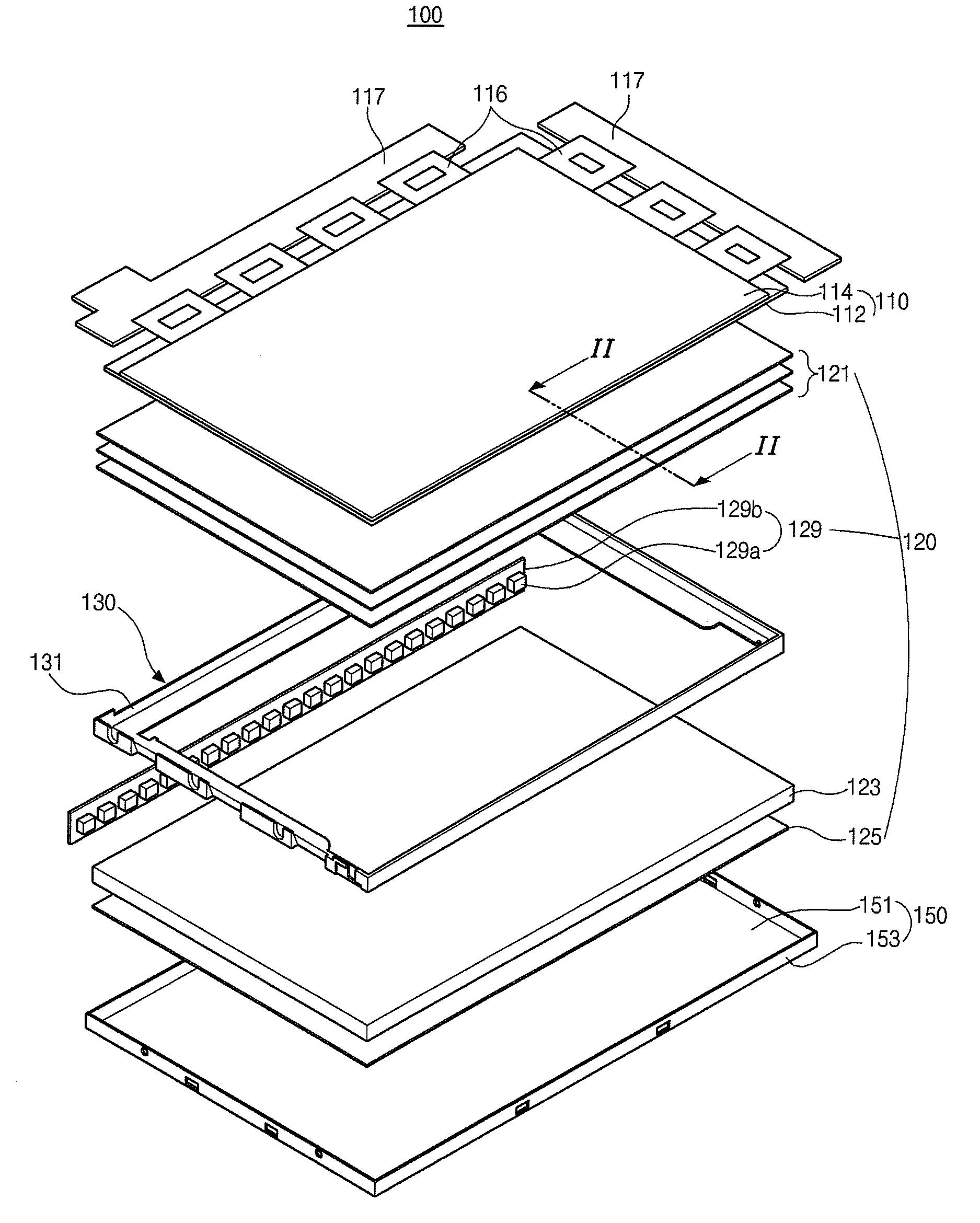
[0033]FIG. 1 is an exploded perspective view showing a liquid crystal display device according to the present invention.

[0034]In FIG. 1, a liquid crystal display (LCD) device 100 includes a liquid crystal panel 110, a backlight unit 120, a main frame 130 and a bottom frame 150. The main frame 130 may be referred to as a guide panel, a main support or a mold frame and the bottom frame 150 may be referred to as a bottom cover or a lower cover. The liquid crystal panel 110 displaying an image includes first and second substrates 112 and 114 facing and spaced apart from each other and a liquid crystal layer (not shown) interposed therebetween.

[0035]Although not shown, when the liquid crystal panel 110 has an active matrix type, a gate line, a data line, a thin film transistor (TFT) and a pixel electrode may be formed on an inner surface of the first substrate 112 referred to as a lower substrate or an array substrate. In addition, a color filter layer, a black matrix and a common electr...

second embodiment

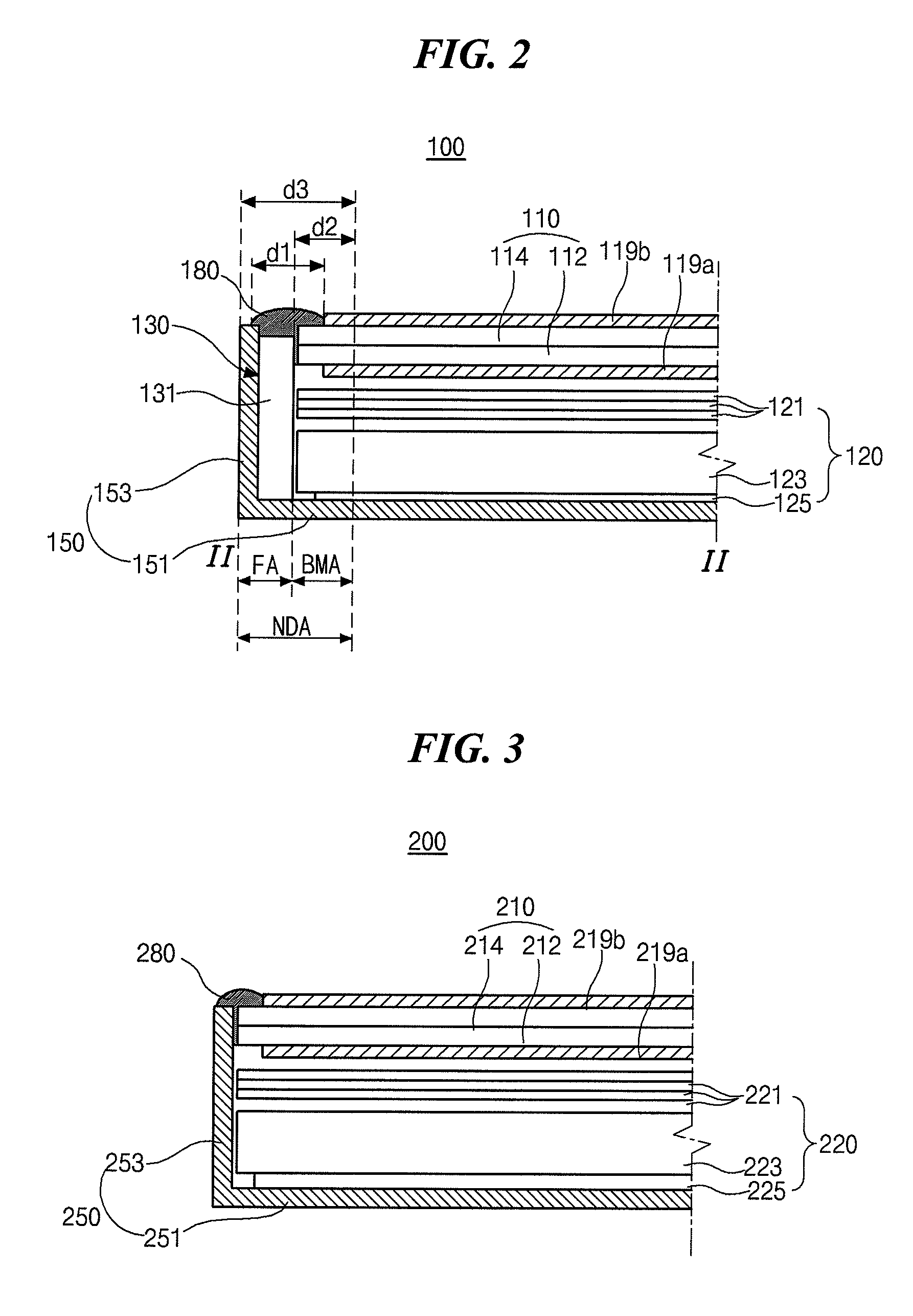
[0059]FIG. 3 is a cross-sectional view showing a liquid crystal display according to the present invention.

[0060]In FIG. 3, a liquid crystal display (LCD) device 200 includes a liquid crystal panel 210, a backlight unit 220 and a bottom frame 250. A reflecting plate 225, a light guide plate 223, a light emitting diode (LED) assembly (not shown) and a plurality of optical sheets 221 constitute the backlight unit 220. In addition, the liquid crystal panel 210 including first and second substrates 212 and 214 and a liquid crystal layer (not shown) therebetween is disposed over the backlight unit 220. First and second polarizing plates 219a and 219b are formed on the outer surfaces of the first and second substrates 212 and 214, respectively.

[0061]The backlight unit 220 and the liquid crystal panel 210 are surrounded by the bottom frame 250 including a horizontal portion 251 and a sidewall portion 253. An edge portion of the liquid crystal panel 210 is attached and fixed to the bottom f...

third embodiment

[0067]FIG. 4 is a cross-sectional view showing a liquid crystal display according to the present invention.

[0068]In FIG. 4, a liquid crystal display (LCD) device 300 includes a liquid crystal panel 310, a backlight unit 320 and a main frame 330. A reflecting plate 325, a light guide plate 323, a light emitting diode (LED) assembly (not shown) and a plurality of optical sheets 321 constitute the backlight unit 320. In addition, the liquid crystal panel 310 including first and second substrates 312 and 314 and a liquid crystal layer (not shown) therebetween is disposed over the backlight unit 320. First and second polarizing plates 319a and 319b are formed on the outer surfaces of the first and second substrates 312 and 314, respectively.

[0069]The backlight unit 320 and the liquid crystal panel 310 are surrounded by the main frame 330 having a rectangular ring shape and including a vertical portion 331. The reflecting plate 325 is attached to the main frame 330 by an attaching member ...


PUM

PropertyMeasurementUnit
widthaaaaaaaaaa
widthaaaaaaaaaa
widthaaaaaaaaaa

Abstract

A display device includes: a display panel displaying an image; a first frame surrounding the display panel; and an adhesive between a side surface of the display panel and a side surface of the first frame, wherein the display device is attached and fixed to the first frame by the adhesive.

Description

[0001]The present application claims the priority benefit of Korean Patent Application No. 10-2011-0074422 filed in Republic of Korea on Jul. 27, 2011 and Korean Patent Application No. 10-2011-0113845 filed in Republic of Korea on Nov. 3, 2011, which are hereby incorporated by reference in their entirety.BACKGROUND[0002]1. Field of the Disclosure[0003]The present disclosure relates to a display device, and more particularly, to a display device including an adhesive that combines a display panel and a frame and preventing a light leakage and a method of fabricating the display device.[0004]2. Discussion of the Related Art[0005]Recently, as information age progresses, demand for display device has increased in various forms. In addition, various flat panel displays (FPDs) having a thin profile, a light weight and a low power consumption such as a liquid crystal display (LCD), a plasma display panel (PDP) and an organic light emitting diode (OLED) have been researched.[0006]Among vari...

Claims


Application Information

Patent Timeline
Patent Type & Authority Applications(United States)
IPC IPC(8): H05K7/00B32B37/12
CPCG02F1/133308G02F2001/133314G02F2001/133317Y10T156/10G02F2001/133325G02F2202/28G02F2001/13332G02F1/133314G02F1/133317G02F1/13332G02F1/133325G02F1/133512G02F1/133528G02F1/133602
Inventor JEONG, HAE-HYEON
Owner LG DISPLAY CO LTD
Why Eureka
Try Eureka