Semiconductor device and method for manufacturing the same

a semiconductor and semiconductor technology, applied in the field of semiconductor devices, can solve the problems of difficult to obtain high overlay accuracy in divided exposures of a region far from the alignment mark, and achieve the effect of high overlay accuracy

Active Publication Date: 2013-02-07
CANON KK
View PDF7 Cites 12 Cited by
  • Summary
  • Abstract
  • Description
  • Claims
  • Application Information

AI Technical Summary

Benefits of technology

[0007]The present invention provides a technique advantageous in manufacturing a large-area semiconductor device with high overlay accuracy while requiring only a small number of steps.

Problems solved by technology

However, it is difficult to obtain high overlay accuracy in divided exposure of a region far from that alignment mark due, for example, to a magnification error and distortion of a projection optical system of an exposure apparatus, expansion / contraction of a substrate, or a driving error of a stage apparatus which positions the substrate.

Method used


Image

  • Semiconductor device and method for manufacturing the same
  • Semiconductor device and method for manufacturing the same
  • Semiconductor device and method for manufacturing the same

Examples


Embodiment Construction

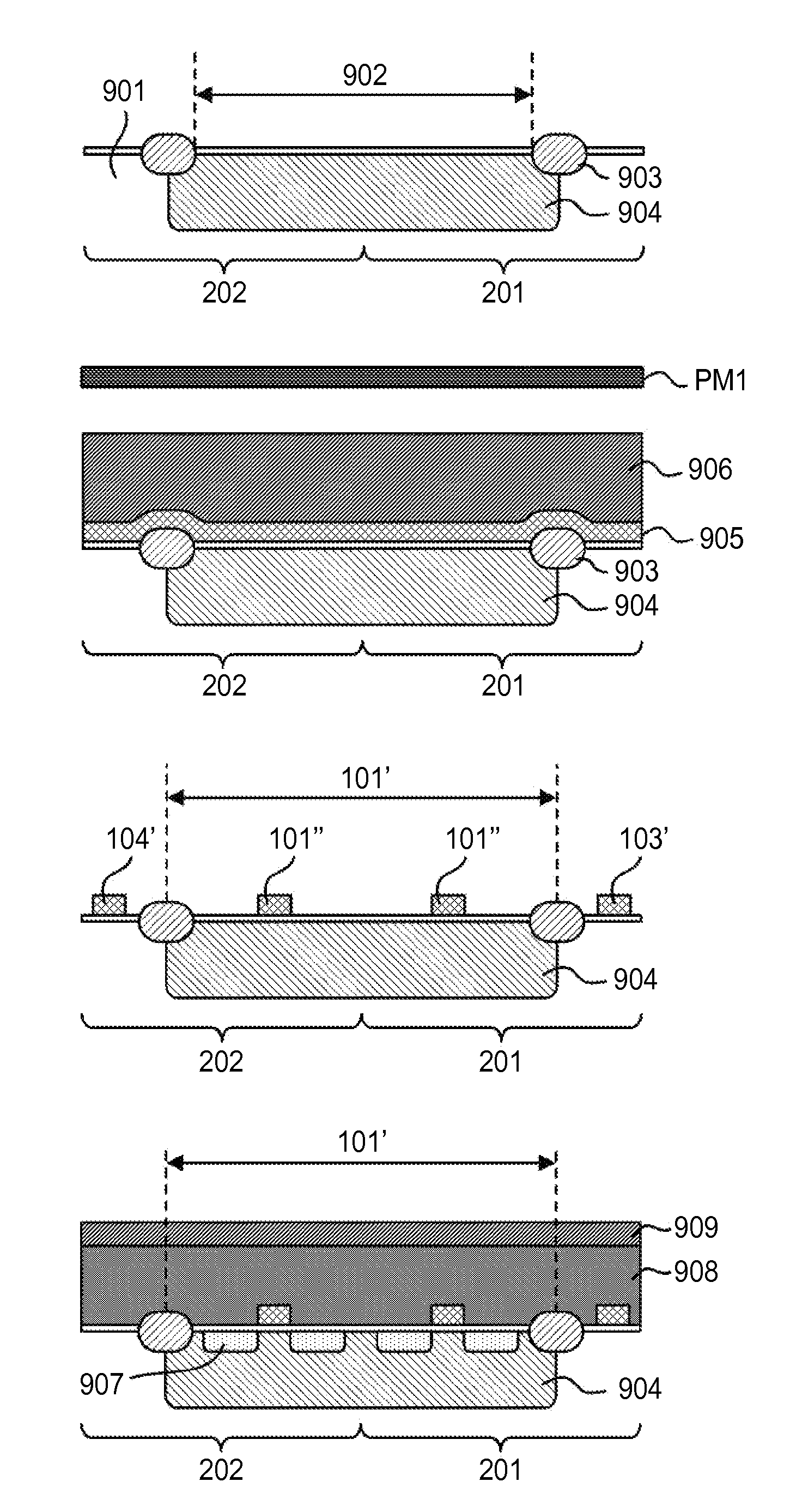
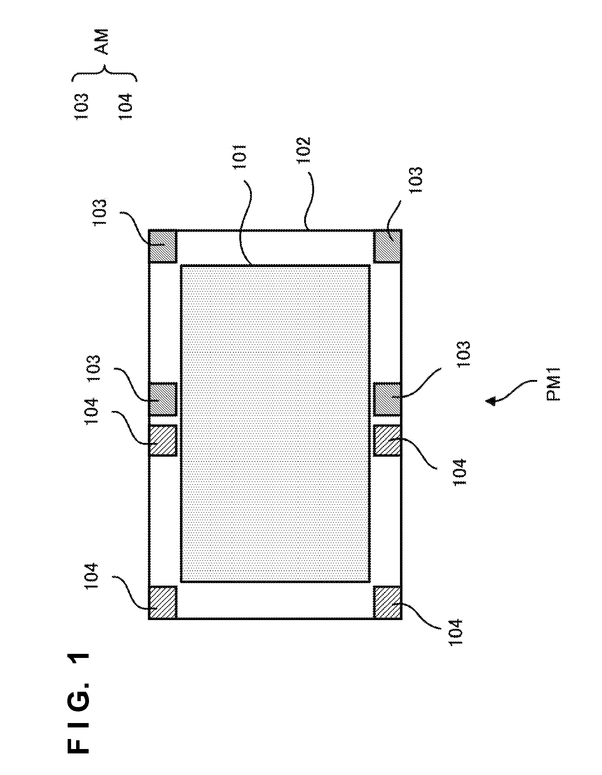
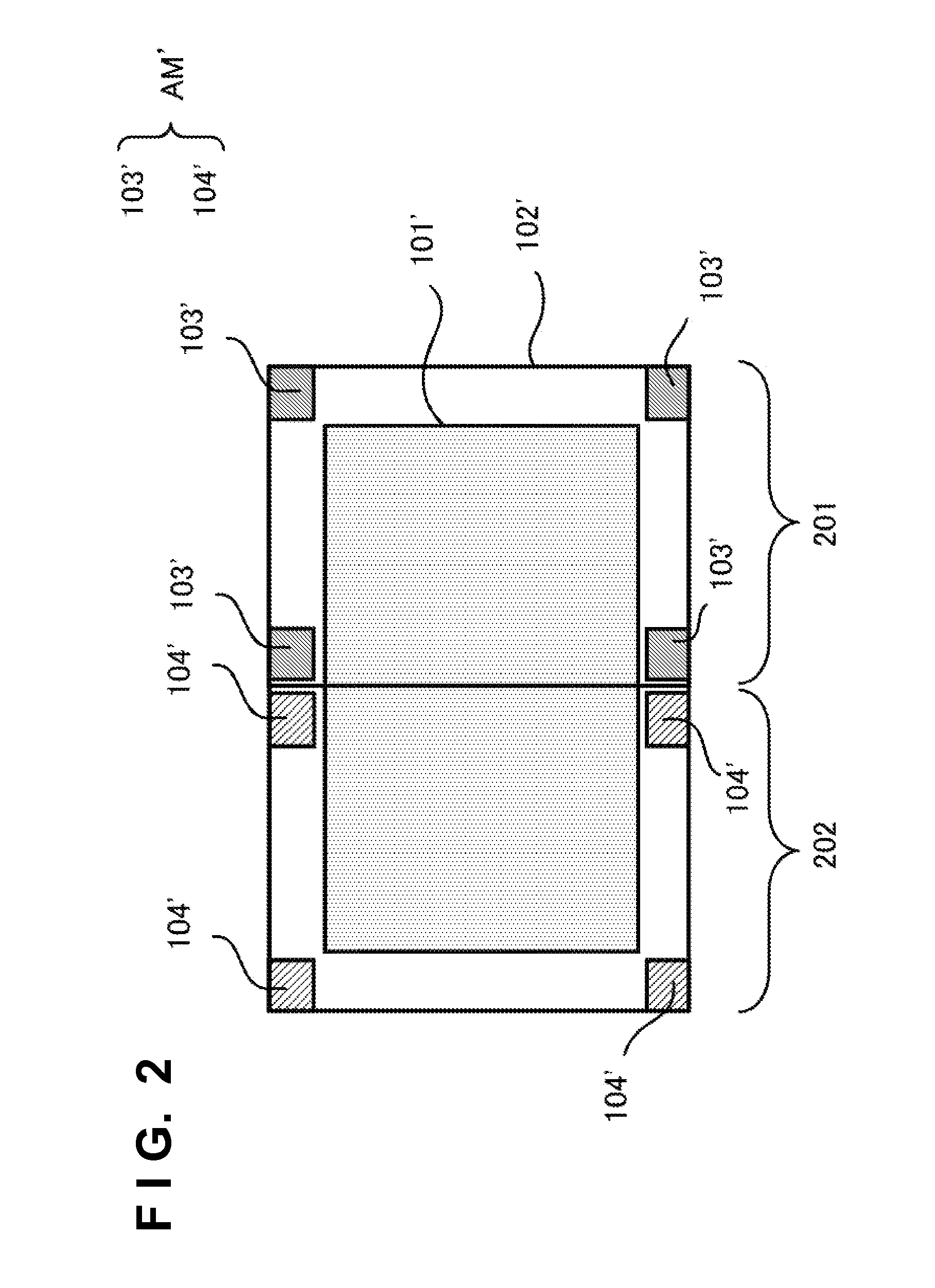
[0019]The first embodiment of the present invention relates to a semiconductor device including a device region in which a circuit element is formed, and a method for manufacturing the same. The manufacturing method according to the first embodiment includes a first photolithography step and a second photolithography step performed after the first photolithography step. The first photolithography step includes a first exposure step of exposing the entire device region on a substrate in one shot, using a first mask including a first pattern and a plurality of first marks. In the first photolithography step, a first device pattern corresponding to the first pattern, and a plurality of alignment marks corresponding to the plurality of first marks are formed in the device region upon the first exposure step. In this case, the substrate includes a first photoresist film formed on a first layer to be patterned, and a latent image of the first pattern and those of the plurality of first ma...


PUM

PropertyMeasurementUnit
structureaaaaaaaaaa
shapeaaaaaaaaaa
timeaaaaaaaaaa

Abstract

A method for manufacturing a semiconductor device includes a first photolithography step of forming a first device pattern corresponding to a first pattern, and a plurality of alignment marks corresponding to a plurality of marks, upon a step of exposing the entire device region in one shot using a first mask including the first pattern and the plurality of marks, and a second photolithography step of, after the first photolithography step, forming second device patterns respectively corresponding to second patterns in a plurality of divided regions which form the device region, upon steps of individually exposing the plurality of divided regions using second masks each including the second pattern corresponding thereto.

Description

BACKGROUND OF THE INVENTION[0001]1. Field of the Invention[0002]The present invention relates to a semiconductor device and a method for manufacturing the same.[0003]2. Description of the Related Art[0004]Japanese Patent Laid-Open No. 2004-111866 discloses a method for manufacturing a semiconductor device by connecting a plurality of patterns to each other by divided exposure so as to form a single-layered pattern. In this manufacturing method, instead of divided exposure, one-shot exposure is used to form a pattern in a layer including a wiring line which exerts a substantial influence on the operation of the semiconductor device depending on the positional relationship with other wiring lines. Japanese Patent Laid-Open No. 2003-248329 discloses divided exposure performed four times while alignment is performed using alignment marks, which are formed on a glass substrate by one-shot exposure using a photomask for forming them.[0005]Japanese Patent Laid-Open No. 2004-111866 neither ...

Claims


Application Information

Patent Timeline
Patent Type & Authority Applications(United States)
IPC IPC(8): G03F7/20H01L23/544
CPCG03F9/7084G03F1/42
Inventor KANOU, TAIKAN
Owner CANON KK
Why Eureka
Try Eureka