Voltage boosting device and voltage boosting circuit

a voltage boosting device and voltage boosting circuit technology, applied in the direction of dc-dc conversion, climate sustainability, power conversion systems, etc., can solve the problems of low conversion efficiency of converting devices, incompatibility with practical requirements, and efficiency reduction, so as to increase conversion efficiency, high voltage gain, and high conversion efficiency

Inactive Publication Date: 2013-02-14
LITE ON TECH CORP +1
View PDF3 Cites 13 Cited by
  • Summary
  • Abstract
  • Description
  • Claims
  • Application Information

AI Technical Summary

Benefits of technology

[0020]The effect of the voltage boosting device of the present invention is to provide low voltage / high current power input, integrated single-stage power conversion that can achieve high voltage gain in a single power conversion process, and having high conversion efficiency. Also, the voltages of the first switch, the second switch and the clamping diodes of the voltage boosting circuit are substantially lower than the conventional voltage boosting circuit. Accordingly, the conducting and switching losses of the circuit elements, and the problem of reverse recovery loss are all substantially reduced to further increase the conversion efficiency.

Problems solved by technology

However, such ways require multiple energy conversions, which lower the conversion efficiency of the converting devices, and do not conform with practical requirements.
Not only does it lower the efficiency, the switching frequency of the power switches S1, S2 cannot be increased, which is necessary to achieve device miniaturization.

Method used


Image

  • Voltage boosting device and voltage boosting circuit
  • Voltage boosting device and voltage boosting circuit
  • Voltage boosting device and voltage boosting circuit

Examples


first embodiment

[0039]FIG. 2 shows the voltage boosting device of the present invention. The voltage boosting device 100 is an interleaved / multiphase-structured voltage booster that can be used in battery charging / discharging systems in hybrid power vehicles, home use direct current micro-grid power generating systems, power factor correctors, high voltage drivers for high intensity discharge (HID) head lights in vehicles, alternative power generating systems that are based on solar energy / wind power / fuel cells, medical electronic instruments, such as X-ray machines, ozone generators, etc.

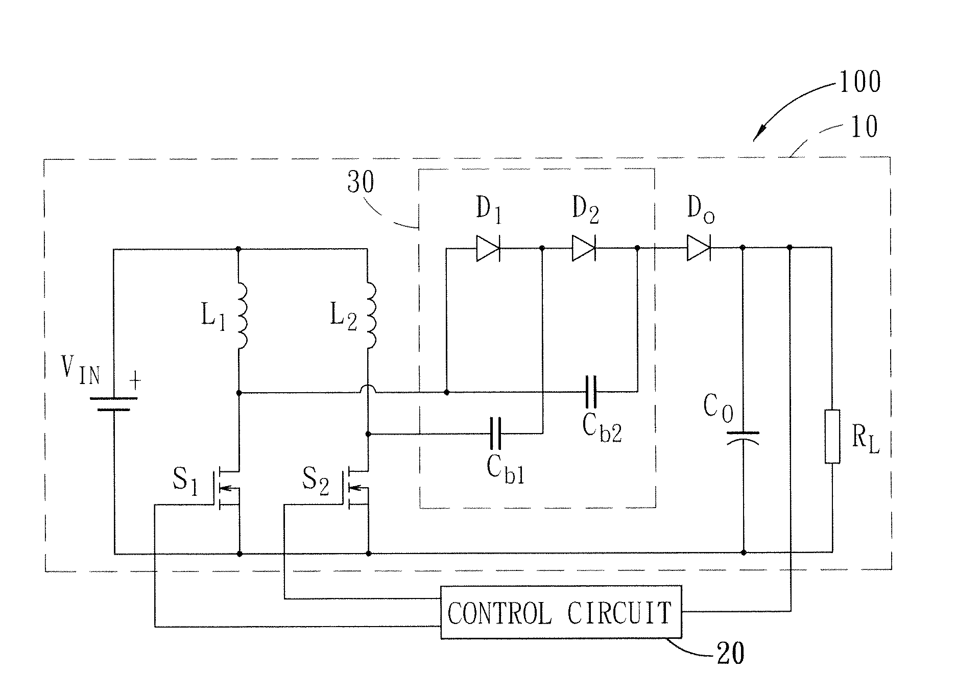
[0040]In the first embodiment, the voltage boosting device 100 receives and boosts a low voltage / high current power source signal VIN to be supplied to electronic devices (i.e., the load RL). The voltage boosting device 100 includes a voltage boosting circuit 10 and a control circuit 20. The voltage boosting circuit 10 includes a first inductor L1, a first switch S1, a second inductor L1, a second switch S2, an au...

second embodiment

[0053]Similarly, when the first switch S1 is not conducting and the second switch S2 conducts, the energy storing element Cb1 of the auxiliary step-up unit 30 can store energy of the first inductor L1, while the second energy storing element Cb2 can release energy to the load RL. When the first switch S1 conducts and the second switch S2 is not conducting, the second energy storing element Cb2 will store energy of the first inductor L1, and the energy of the first energy storing element Cb1 and the stored energy of the second inductor L2 are released together to the load RL, thus achieving the goal of boosting the input power source signal VIN. The voltage boosting circuit 10 of the second embodiment has the voltage gain as follows:

31-D

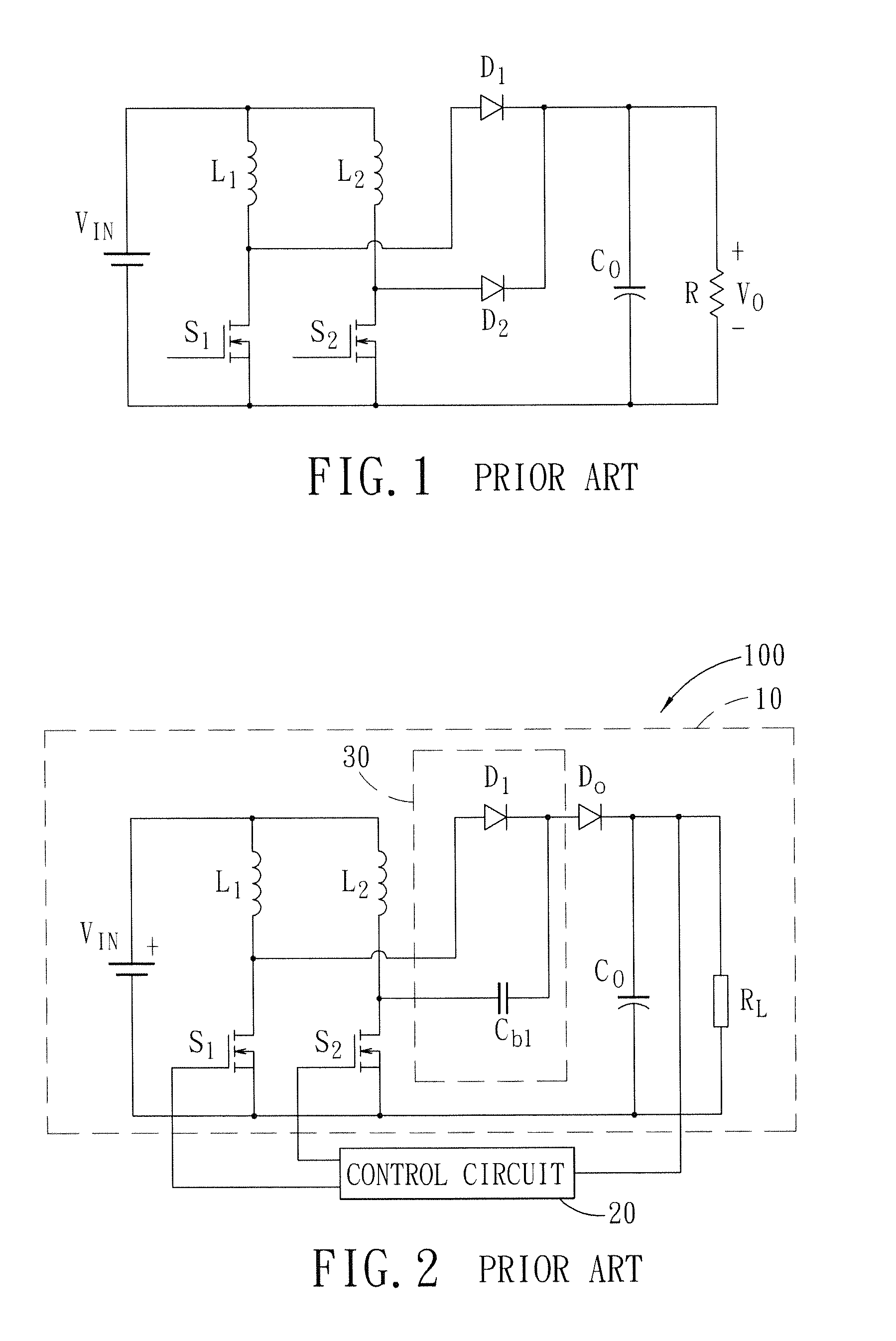
[0054]FIG. 7 shows the third embodiment of the voltage boosting device 100 of the present invention. The difference between the first embodiment and the third embodiment resides in that the auxiliary step-up unit 30 can include multiple clamping diode...

third embodiment

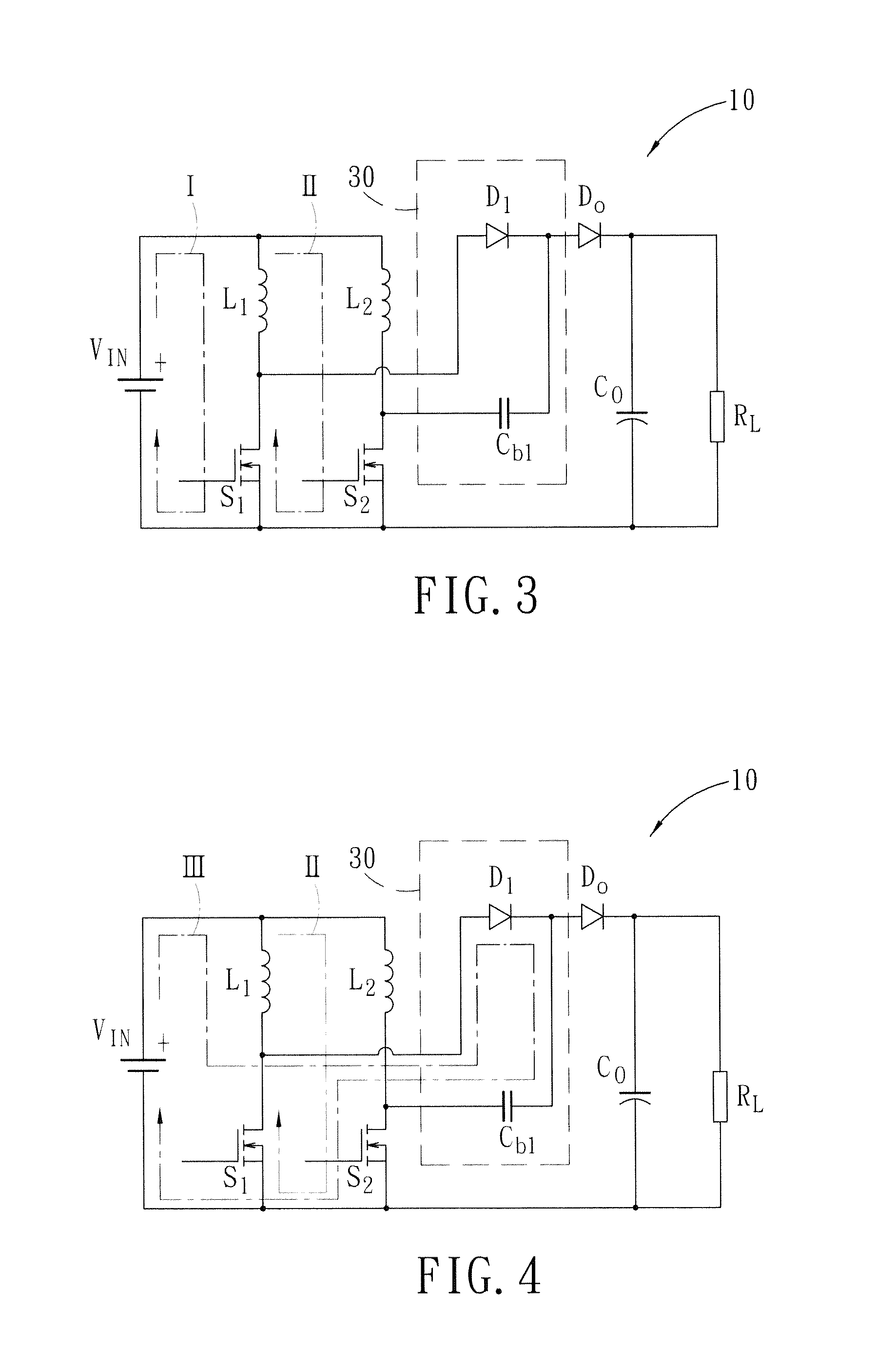
[0059]When the first switch S1 conducts and the second switch S2 is not conducting, the energy storing elements electrically coupled to the junction of the second inductor L2 and the second switch S2 (the first and third energy storing elements Cb1, Cb3) will release energy to the output capacitor CO, and the energy storing element electrically coupled to the junction of the first inductor L1 and the first switch S1 (the second energy storing element Cb2) will store energy of the first inductor L1. Thus, the goal of boosting the input power source signal VIN is achieved, and the voltage boosting circuit 10 of the third embodiment has the voltage gain as follows:

41-D

[0060]FIG. 8 is a characteristic curve plot illustrating voltage gains of the conventional interleaved voltage boosting circuit and the three embodiments of the voltage boosting circuit 10 of the present invention. The horizontal axis represents the duty cycles of the first and second switches S1, S2, and the vertical axi...


PUM


Abstract

A voltage boosting circuit includes a first inductor, a first switch, a second inductor, a second switch, a first clamping diode, and a first energy storing element. When the first switch and the second switch conduct, the first and second inductors are able to store energy of a power source signal. When the first switch is not conducting and the second switch conducts, the first inductor is able to release energy to the first energy storing element. When the first switch conducts and the second switch is not conducting, the second inductor and the first energy storing element are able to release energy to a load.

Description

CROSS-REFERENCE TO RELATED APPLICATION[0001]This application claims priority to Chinese Application No. 201110234341.1, filed on Aug. 12, 2011.BACKGROUND OF THE INVENTION[0002]1. Field of the Invention[0003]The invention relates to a voltage boosting device, and more particularly to a voltage boosting device with a high voltage gain.[0004]2. Description of the Related Art[0005]With petrol prices constantly rising and the topic of environmental conservation constantly being addressed in recent years, many countries have been aggressively promoting development of distributed power generating systems. As distributed power generation devices have the characteristic of low voltage output, they are widely used in storage devices such as photovoltaic batteries, fuel cells, storage batteries, wind turbines, etc.[0006]With different applications and to achieve the requirement for high voltage boost in distributed power generating devices, there are ways incorporating two-stage or series-conn...

Claims


Application Information

Patent Timeline
Patent Type & Authority Applications(United States)
IPC IPC(8): H02M7/00
CPCY02B10/30H02M3/158H02M1/0095
Inventor LAI, CHING-MING
Owner LITE ON TECH CORP
Why Eureka
Try Eureka