Non-volatile static random access memory devices and methods of operations

a random access memory and non-volatile technology, applied in static storage, information storage, digital storage, etc., can solve the problems of increasing the number of transistor elements, less compact and less efficient approach, and adding more operational complexity

Active Publication Date: 2013-02-14
SYNERGER INC
View PDF8 Cites 6 Cited by
  • Summary
  • Abstract
  • Description
  • Claims
  • Application Information

AI Technical Summary

Benefits of technology

[0002]This invention relates to Non-Volatile Static Random Access Memory (NVSRAM) and the methods of operations. In particular, only one single non-volatile element embedded in a conventional SRAM cell forms an NVSRAM cell device of the invention. A plurality of NVSRAM cell devices of the invention can be integrated into a compact memory array. Due to a new configuration of the NVSRAM device of the invention, switching elements in the conventional NVSRAM devices to isolate the SRAM cell from the high voltages of writing and erase operations of the non-volatile element are omitted. The operations of the NVSRAM cells of the invention are also simplified. The NVSRAM device of the invention has a read / write speed of a conventional SRAM and non-volatile property of a non-volatile memory cell.

Problems solved by technology

However, this approach is less compact and less efficient due to the two separated non-volatile memory array and SRAM array with peripheral circuitries.
This is due to the incompatibility of high / low voltage operations of volatile and non-volatile cell devices.
In terms, those approaches increase the numbers of transistor elements and add more operational complexity.
In general the Metal-Oxide-Semiconductor Field Effect Transistors (MOSFETs) in SRAM cells are designed for low voltage operations based on the performance and size considerations, and incompatible with the high voltage program / erase operations of non-volatile elements.

Method used


Image

  • Non-volatile static random access memory devices and methods of operations
  • Non-volatile static random access memory devices and methods of operations
  • Non-volatile static random access memory devices and methods of operations

Examples


Embodiment Construction

[0024]The following detailed description is meant to be illustrative only and not limiting. It is to be understood that other embodiment may be utilized and structural changes may be made without departing from the scope of the present invention. Also, it is to be understood that the phraseology and terminology used herein are for the purpose of description and should not be regarded as limiting. Those of ordinary skill in the art will immediately realize that the embodiments of the present invention described herein in the context of methods and schematics are illustrative only and are not intended to be in any way limiting. Other embodiments of the present invention will readily suggest themselves to such skilled persons having the benefits of this disclosure.

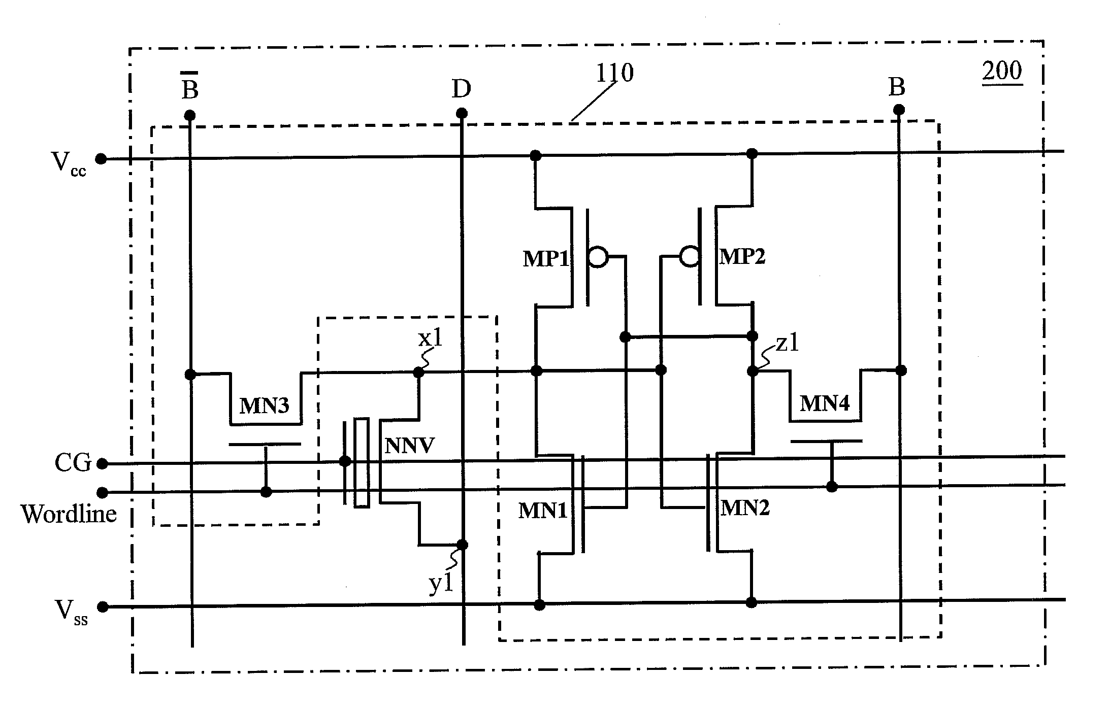
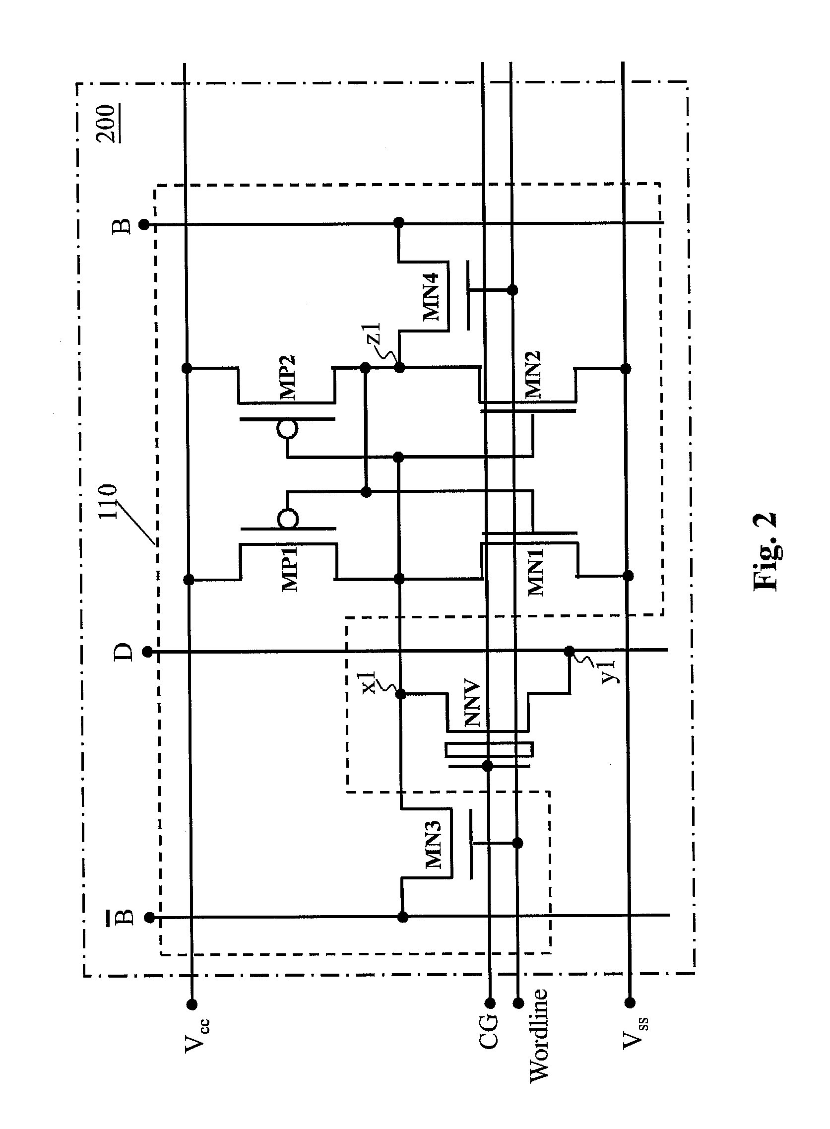
[0025]The NVSRAM cell 200 for an N-type non-volatile element NV embedded in 6T SRAM cell 110 (MP1, MP2, MN1, MN2, MN3, and MN4) is shown in FIG. 2. One node x1 of the N-type non-volatile element NV is connected to the output ...


PUM


Abstract

Non-Volatile Static Random Access Memory (NVSRAM) cell devices applying only one single non-volatile element embedded in a conventional Static Random Access Memory (SRAM) cell are disclosed. The NVSRAM cell devices can be integrated into a compact cell array. The NVSRAM devices of the invention have a read / write speed of a conventional SRAM and non-volatile property of a non-volatile memory cell. The methods of operations for the NVSRAM devices of the invention are also disclosed.

Description

BACKGROUND OF THE INVENTION[0001]1. Field of the invention[0002]This invention relates to Non-Volatile Static Random Access Memory (NVSRAM) and the methods of operations. In particular, only one single non-volatile element embedded in a conventional SRAM cell forms an NVSRAM cell device of the invention. A plurality of NVSRAM cell devices of the invention can be integrated into a compact memory array. Due to a new configuration of the NVSRAM device of the invention, switching elements in the conventional NVSRAM devices to isolate the SRAM cell from the high voltages of writing and erase operations of the non-volatile element are omitted. The operations of the NVSRAM cells of the invention are also simplified. The NVSRAM device of the invention has a read / write speed of a conventional SRAM and non-volatile property of a non-volatile memory cell.[0003]2. Description of the Related Art[0004]Semiconductor memories have been broadly applied to electronic systems. Electronic systems requi...

Claims


Application Information

Patent Timeline
Patent Type & Authority Applications(United States)
IPC IPC(8): G11C14/00
CPCG11C14/0063G11C14/0054G11C11/41G11C11/413
Inventor WANG, LEE
Owner SYNERGER INC
Why Eureka
Try Eureka