Method of simulating an ESD circuit layout

Inactive Publication Date: 2013-02-14
HIMAX TECH LTD
View PDF2 Cites 3 Cited by
  • Summary
  • Abstract
  • Description
  • Claims
  • Application Information

AI Technical Summary

Benefits of technology

[0008]In view of the foregoing, it is an object of the embodiment of the present invention to provide a method of simulating an electrostatic discharge (ESD) circuit layout th

Problems solved by technology

Electrostatic discharge (ESD) is harmful to integrated circuits made of semiconductor materials such as silicon and silicon oxide, which may be permanently damaged by a sudden and brief current or voltage.
Unfortunately, most test schemes fail to opportunely iden

Method used


Image

  • Method of simulating an ESD circuit layout
  • Method of simulating an ESD circuit layout
  • Method of simulating an ESD circuit layout

Examples


Embodiment Construction

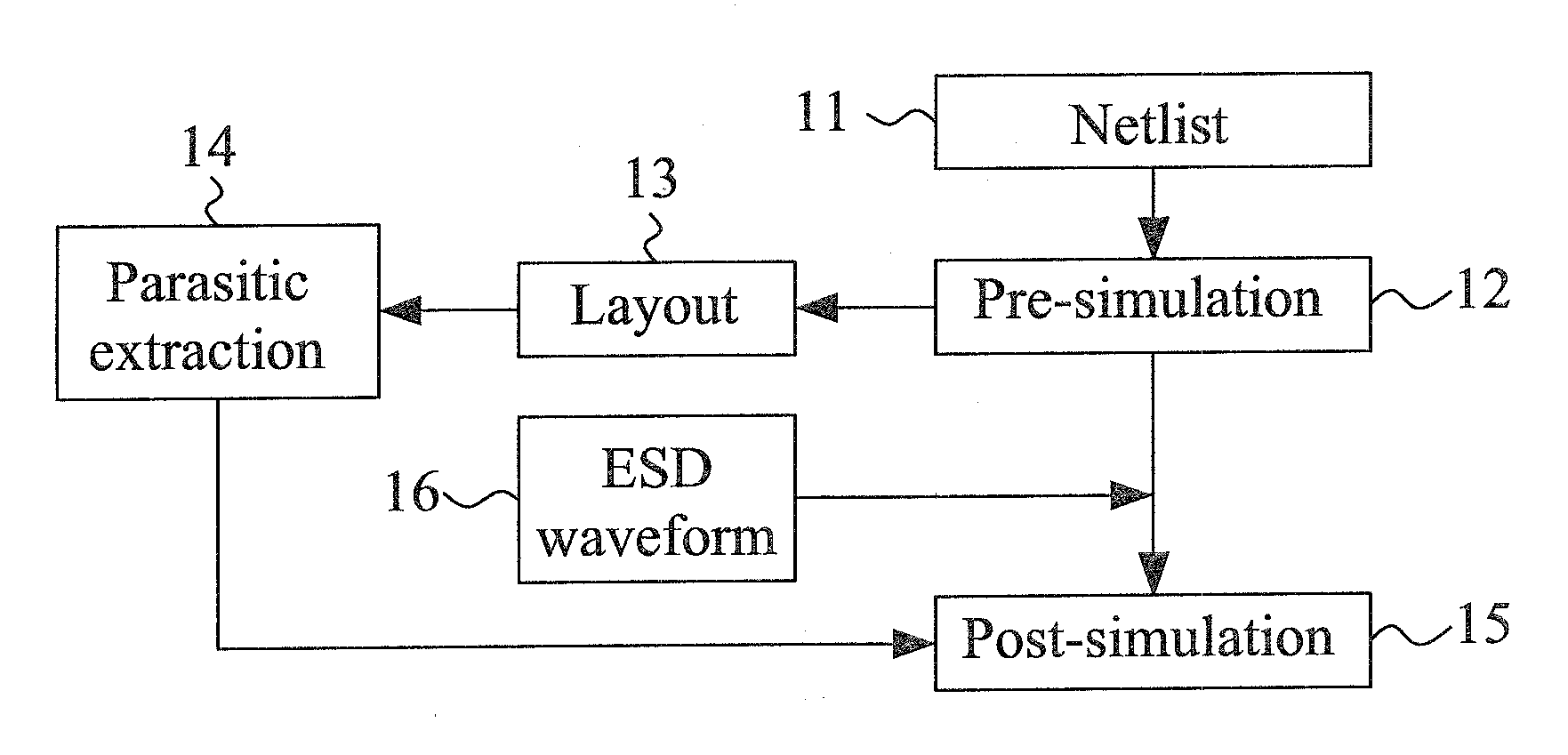
[0014]Referring more particularly to the drawings, FIG. 1 is a flow diagram illustrating a method of simulating an electrostatic discharge (ESD) circuit layout according to one embodiment of the present invention.

[0015]In step 11, a netlist that describes the connectivity among components (or instances) in an electronic circuit is first provided. Next, in step 12, the netlist is fed to a transistor-level circuit simulation tool, such as HSIM provided by Synopsys, Inc., for modeling of circuit operation in order to simulate (or verify) a circuit's behavior. In the specification, the verification performed in step 12 is also called pre-simulation (or simply pre-sim).

[0016]Subsequently, in step 13, the result of the pre-simulation is utilized to generate a circuit layout (including an ESD circuit layout), which is represented in terms of shapes that correspond to patterns of a variety of layers making up the circuit. The layers in fabricating semiconductor devices are commonly classifi...


PUM


Abstract

A method of simulating an electrostatic discharge (ESD) circuit layout is disclosed. A netlist of an electronic circuit is pre-simulated. A circuit layout, including an ESD circuit layout, is accordingly generated. Parasitic is extracted according to the generated circuit layout. The ESD circuit layout is post-simulated according to an ESD waveform and a result of the parasitic extraction.

Description

BACKGROUND OF THE INVENTION[0001]1. Field of the Invention[0002]The present invention generally relates to electrostatic discharge (ESD), and more particularly to a simulation method for an ESD circuit layout.[0003]2. Description of Related Art[0004]Electrostatic discharge (ESD) is harmful to integrated circuits made of semiconductor materials such as silicon and silicon oxide, which may be permanently damaged by a sudden and brief current or voltage. Accordingly, integrated circuits are commonly equipped with ESD protection circuits and need to be subjected to various ESD tests during their designing and manufacturing processes for verifying their resistance level or insusceptibility to ESD. The human-body model (HBM) is one commonly used test model for characterizing ESD that imitates a human's touch on an integrated circuit, and machine model (MM) is another one that imitates a machine's contact with the integrated circuit.[0005]As those in the field well know, it is most advanta...

Claims


Application Information

Patent Timeline
IPC IPC(8): G06F17/50
CPCG06F17/5063G06F30/36
Inventor TSAI, CHING-LINGCHEN, SHIH-FAN
Owner HIMAX TECH LTD
Why Eureka
Try Eureka