Long Wavelength Infrared Superlattice

a superlattice and infrared technology, applied in the field of semiconductor materials fabrication, can solve the problems of narrow design parameters of realized devices, and achieve the effect of extending the cutoff wavelength and reducing the loss of superlattice quality

Inactive Publication Date: 2013-02-21
SVT ASSOCS
View PDF4 Cites 21 Cited by
  • Summary
  • Abstract
  • Description
  • Claims
  • Application Information

AI Technical Summary

Benefits of technology

[0019]Both experimental data and theoretical analysis by the present inventors [reference 6] show that InSb layers play an important role in type-II superlattice structure, especially for operation in the LWIR portion of the electromagnetic spectrum. In particular, adjusting the optical cutoff wavelength of the superlattice by varying the InSb thickness is a much more effective means than by varying the thickness of InAs or GaSb constituent layers. The present invention is a new design for a type-II superlattice which incorporates thicker InSb layers, whose function is to extend the cutoff wavelength, and a thin GaAsSb (gallium arsenide antimonide) intralayer inserted into InAs layers, which serves to balance the subsequent strain introduced by the aforementioned InSb layers. The application of GaAsSb intralayers within the superlattice overcomes the loss of superlattice quality due to the strain forces induced by the incorporation of InSb layers.

Problems solved by technology

This limitation of specific layers with which to form the type-II superlattice creates a narrowed constraint in the design parameters of the realized device.

Method used


Image

  • Long Wavelength Infrared Superlattice
  • Long Wavelength Infrared Superlattice
  • Long Wavelength Infrared Superlattice

Examples


example

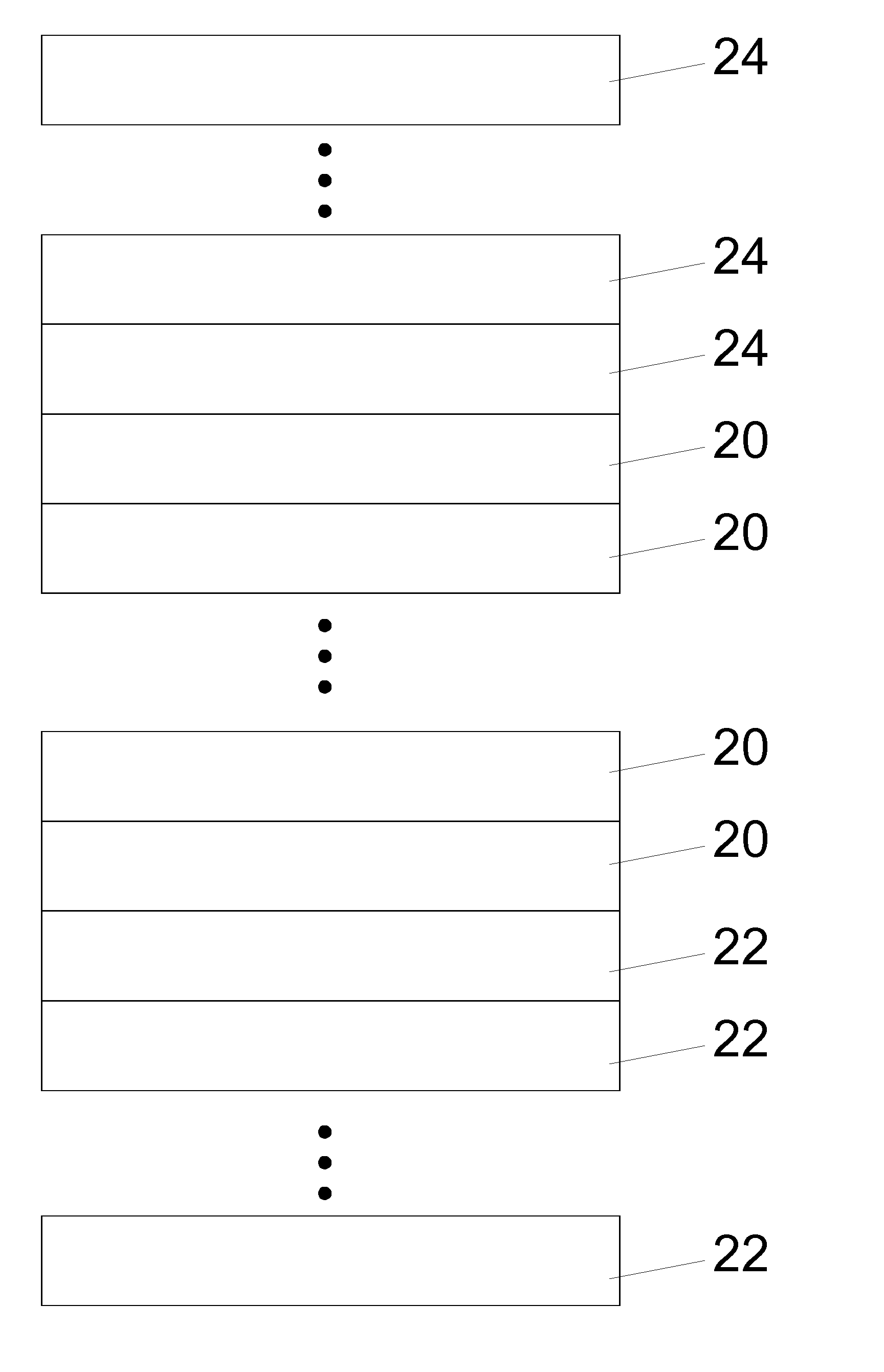
[0047]The present invention need not be necessarily actualized by a particular growth method, nor is realization limited to a specific host substrate. However the following discussion will present an example on how to apply the novel type-II superlattice of the present invention to the creation of an infrared detector structure.

[0048]The type-II superlattice may be epitaxially grown using the molecular beam epitaxy (MBE) technique. In this method high purity elemental material, such as In, Ga, As, Sb, Si and Be are individually isolated within a high vacuum chamber. Each elemental source is individually heated, creating a vapor composed of that element. The vapors can then be individually directed toward the growth substrate for specific and deliberate time duration, where the vapors recombine on the substrate surface and form the desired semiconductor material.

[0049]A p-type GaSb host substrate may be loaded into the growth chamber of this MBE system. The GaSb substrate is heated i...


PUM

PropertyMeasurementUnit
thicknessaaaaaaaaaa
thicknessaaaaaaaaaa
total thicknessaaaaaaaaaa

Abstract

An embodiment of the present invention improves the fabrication and operational characteristics of a type-II superlattice material. Layers of indium arsenide and gallium antimonide comprise the bulk of the superlattice structure. One or more layers of indium antimonide are added to unit cells of the superlattice to provide a further degree of freedom in the design for adjusting the effective bandgap energy of the superlattice. One or more layers of gallium arsenide antimonide are added to unit cells of the superlattice to counterbalance the crystal lattice strain forces introduced by the aforementioned indium antimonide layers.

Description

CROSS-REFERENCE TO RELATED APPLICATIONS[0001]This application claims the benefit of the U.S. Provisional application Ser. No. 61 / 525,500, filed 2011 Aug. 19 by the present inventors.FEDERALLY SPONSORED RESEARCH [0002]Not ApplicableSEQUENCE LISTING OR PROGRAM [0003]Not ApplicableBACKGROUND [0004]1. Field of the Invention[0005]The present invention relates to the fabrication of semiconductor materials for application in optoelectronic devices operating in the infrared portion of the electromagnetic spectrum. Specifically, the repeated and deliberate deposition of thin semiconductor layers such as indium arsenide (InAs), indium antimonide (InSb), gallium arsenide antimonide (GaAsSb) or gallium antimonide (GaSb), not necessarily in this order, comprises a superlattice. This superlattice exhibits specific material properties, such as effective semiconductor bandgap energy, and these properties may be tailored by changing the individual layer thicknesses and / or layer constituents comprisi...

Claims


Application Information

Patent Timeline
Patent Type & Authority Applications(United States)
IPC IPC(8): H01L29/06
CPCH01L21/02398H01L21/02463H01L21/02466H01L21/02505H01L21/02507B82Y20/00H01L21/02549H01L29/155H01L29/20H01L31/035236H01L21/02546
Inventor CHEN, YIQIAOCHOW, PETER
Owner SVT ASSOCS
Why Eureka
Try Eureka