
Early noise detection and noise aware routing in circuit design

a technology of noise detection and routing, applied in the direction of computer aided design, program control, instruments, etc., can solve problems such as noise reduction actions, and achieve the effect of higher priority

Inactive Publication Date: 2013-02-21
GLOBALFOUNDRIES INC
View PDF2 Cites 9 Cited by
  • Summary
  • Abstract
  • Description
  • Claims
  • Application Information

AI Technical Summary

Benefits of technology

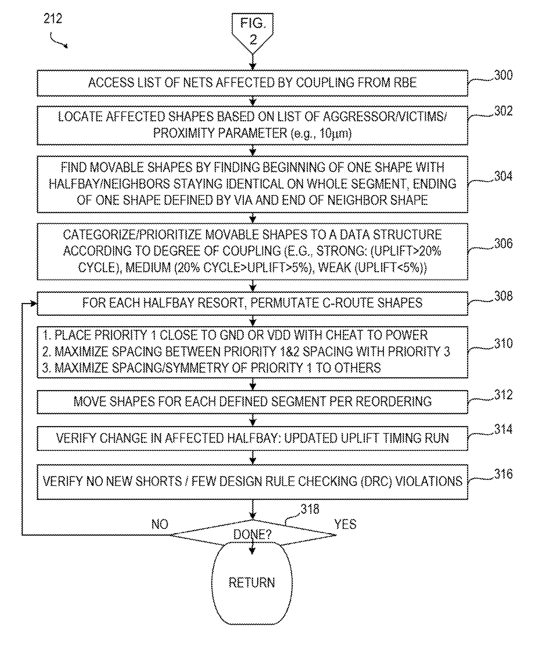
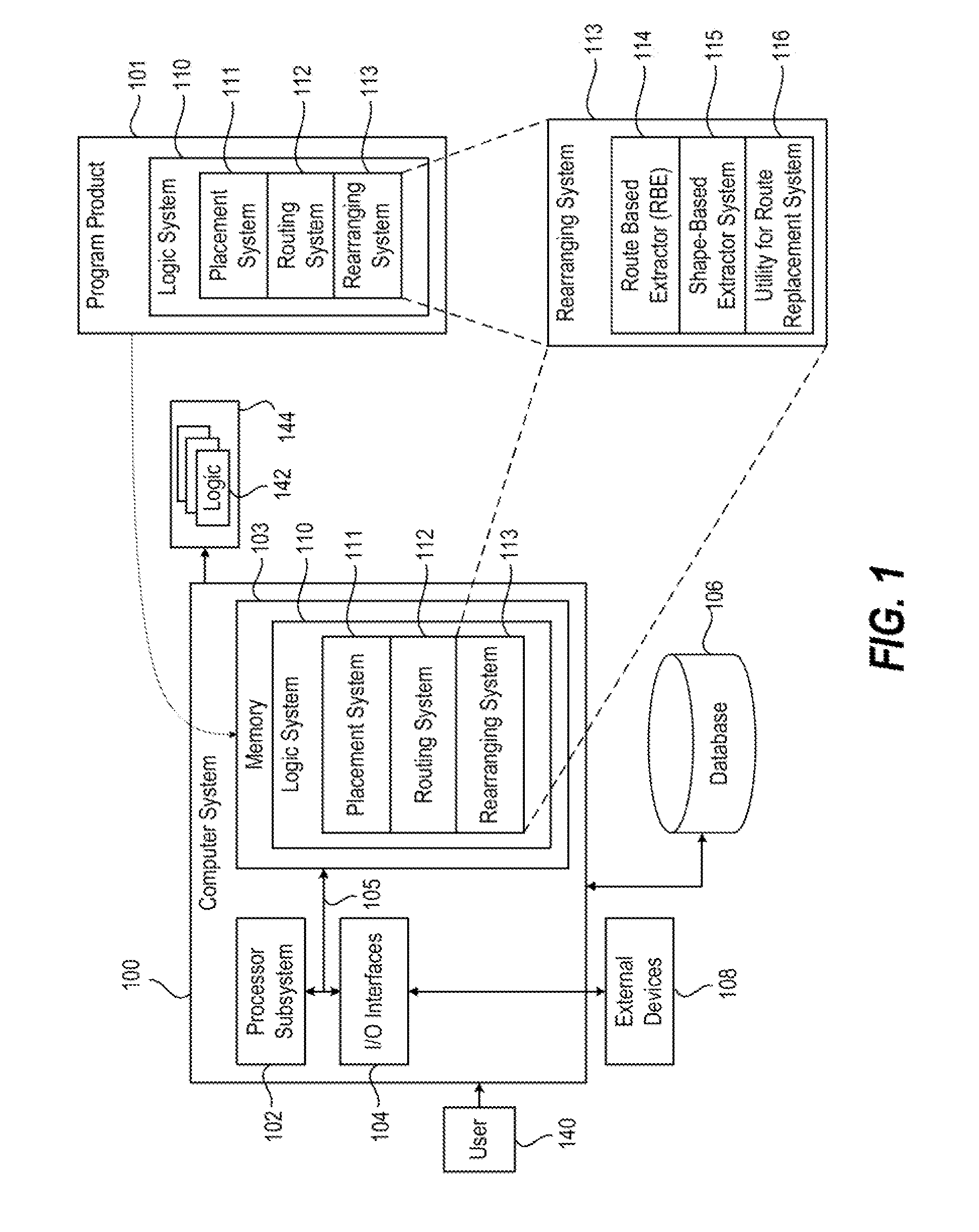
The patent describes a method, system, and computer program for improving the wiring of an integrated circuit design to reduce noise caused by coupled wires. By rearranging certain wires within a specific area, noise is minimized and the performance of the circuit is improved. This technique involves moving wires that are affected by noise to a separate area between a ground stripe and an adjacent voltage stripe, which reduces the impact of noise on other parts of the circuit.

Problems solved by technology

During routing, the router has no knowledge about timing and switching of the signals and thus cannot take noise reduction actions at this early stage of physical design.

Method used


Image

  • Early noise detection and noise aware routing in circuit design
  • Early noise detection and noise aware routing in circuit design
  • Early noise detection and noise aware routing in circuit design

Examples


Embodiment Construction

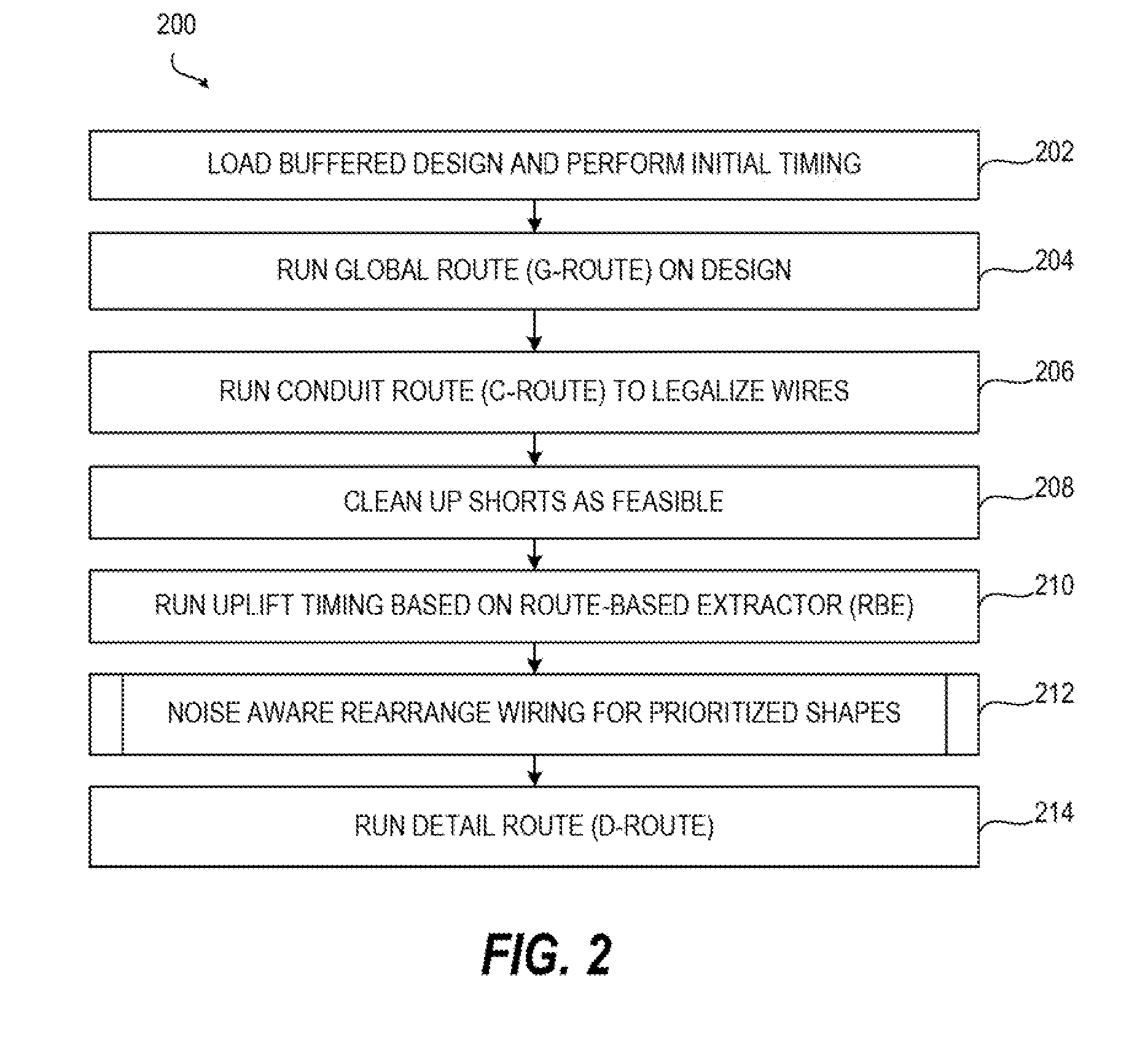
[0019]The illustrative embodiments provide a computerized method, data processing system and computer program product to reduce noise for a buffered design of an electronic circuit which has already been placed and routed. For all areas between a power (vdd) stripe and a ground (gnd) stripe, that is a half bay, in the design, the shapes are divided in different criticality levels. The shapes are rearranged based on their criticality level such that shapes with higher criticality level are placed closer to the gnd or vdd stripes than those with lower criticality level. Thereby, the present innovation avoids a time-consuming and error-prone manual approach to rearranging the shapes.

[0020]In the following detailed description of exemplary embodiments of the innovation, specific exemplary embodiments in which the innovation may be practiced are described in sufficient detail to enable those skilled in the art to practice the innovation, and it is to be understood that other embodiments ...


PUM


Abstract

A computerized method, data processing system and computer program product reduce noise for a buffered design of an electronic circuit which was already placed and routed. For all areas between a power stripe and a ground stripe (half bay) in the design, the shapes are divided in different criticality levels. The shapes are rearranged based on their criticality level such that shapes with higher criticality level are placed closer to the stripes than those with lower criticality level.

Description

BACKGROUND[0001]1. Technical Field[0002]The present disclosure relates to the design of very large scale integrated (VLSI) circuits, and more particularly to improved routing of electric circuits on an integrated circuit chip to avoid noise coupling in noise sensitive areas.[0003]2. Description of the Related Art[0004]In the manufacture of microelectronics, circuits and other logic must be placed on chips and routed under certain wireability and timing constraints. Specifically, the electric circuits must be placed and routed in such a way that all wiring corresponding to the nets joining the electric circuits can be placed and connected as required. As a rule, routing begins after a floor plan has been laid out and the electric circuits have been placed on the chip. Routing is generally split into a global routing step followed by a detailed routing step. During global routing, a complete set of instructions is provided according to which the detailed router is to place actual wiri...

Claims


Application Information

Patent Timeline
Patent Type & Authority Applications(United States)
IPC IPC(8): G06F17/50
CPCG06F2217/82G06F17/5077G06F30/394G06F2119/10
Inventor DAELLENBACH, LUKASGAUGLER, ELMARHALLER, WILHELMRICHTER, RALF
Owner GLOBALFOUNDRIES INC
Learn More