Method of manufacturing multilayer printed circuit board

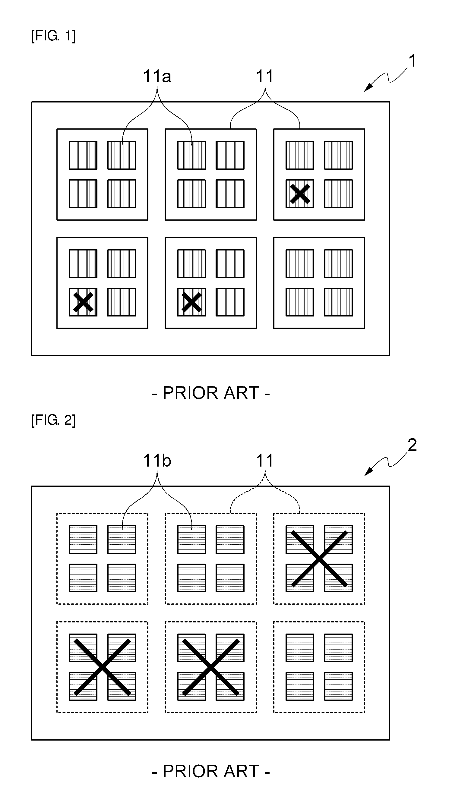
a printed circuit board and multi-layer technology, applied in the field of multi-layer printed circuit board manufacturing, can solve the problems of multi-layer pcb, loss of yield, loss of yield, etc., and achieve the effects of preventing product loss, reducing manufacturing costs, and improving productivity

Inactive Publication Date: 2013-02-28
SAMSUNG ELECTRO MECHANICS CO LTD
View PDF3 Cites 0 Cited by
  • Summary
  • Abstract
  • Description
  • Claims
  • Application Information

AI Technical Summary

Benefits of technology

[0014]The present invention has been invented in order to overcome the above-described problems and it is, therefore, an object of the present invention to provide a method of manufacturing a multilayer PCB that is capable of improving productivity and reducing manufacturing costs by preventing product loss due to disposal of a PCB unit having a defective inner layer circuit pattern portion at the time of failure of the existing inner layer circuit pattern portion.
[0015]It is another object of the present invention to provide a method of manufacturing a multilayer PCB that is capable of further improving workability and productivity and reducing manufacturing costs by performing post-processes such as formation of an outer layer circuit pattern portion in a state in which a plurality of PCB units having only good inner layer circuit pattern portions are arrayed on a working panel.

Problems solved by technology

However, a conventional method of manufacturing a multilayer PCB has the following problems.
At this time, when at least one of the inner layer circuit pattern portions 11a is determined as defective, since the PCB unit having the inner layer circuit pattern portion determined as defective should be scrapped or the entire inner layer PCB sheet should be scrapped, there is a problem of loss of yield.
So there is a problem of loss of yield.
Therefore, the conventional method of manufacturing a multilayer PCB has a problem of deterioration of productivity and workability.
Accordingly, there is a problem of increase in manufacturing costs.

Method used


Image

  • Method of manufacturing multilayer printed circuit board
  • Method of manufacturing multilayer printed circuit board
  • Method of manufacturing multilayer printed circuit board

Examples


Embodiment Construction

[0029]Hereinafter, preferable embodiments of the present invention to achieve the above-described objects will be described with reference to the accompanying drawings. In this description, the same elements are represented by the same names and the same reference numerals, and additional description which is repeated or limits interpretation of the meaning of the invention may be omitted.

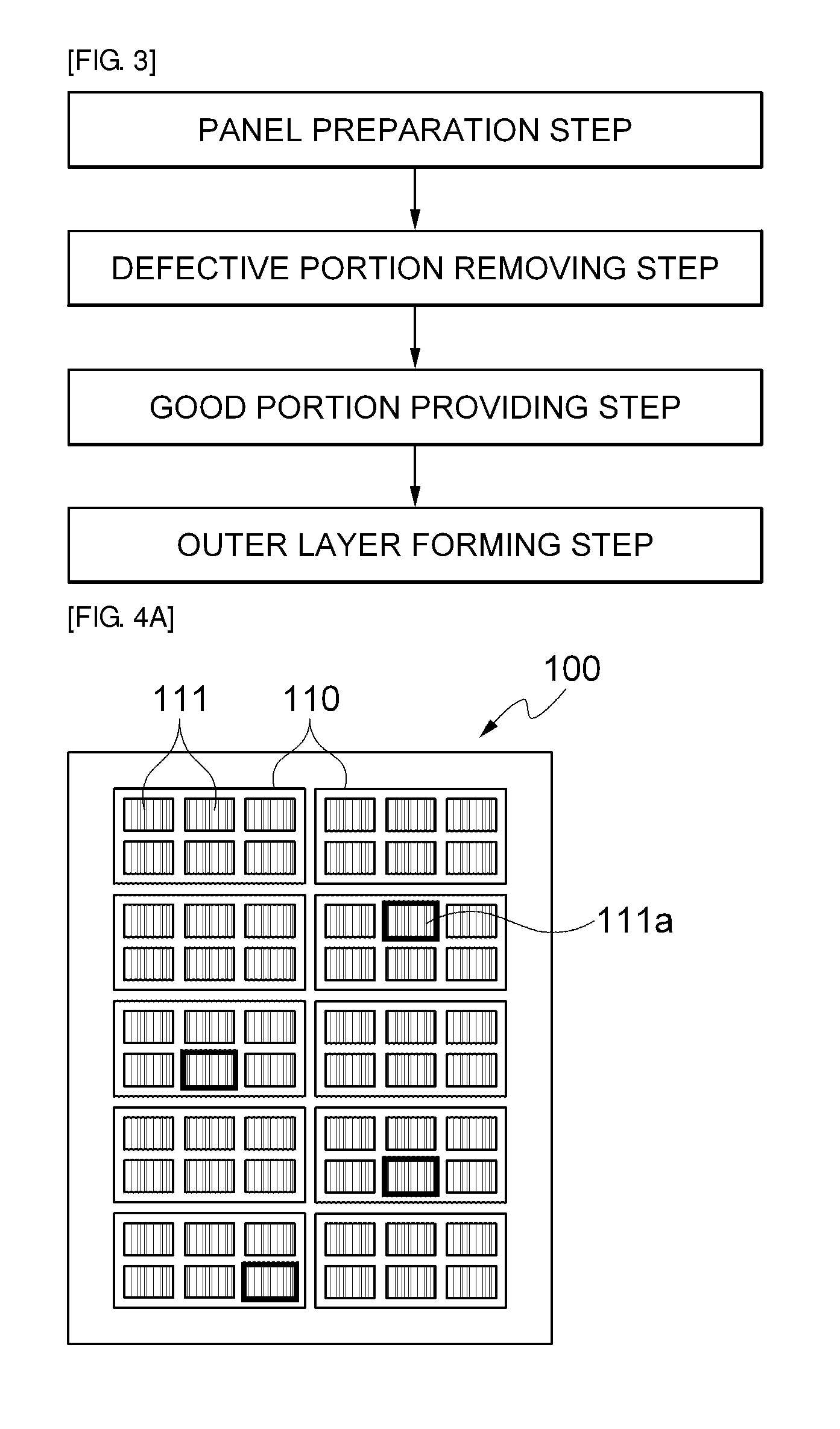
[0030]First, an embodiment of a method of manufacturing a multilayer PCB in accordance with the present invention will be described in detail with reference to the accompanying FIGS. 3 to 4e.

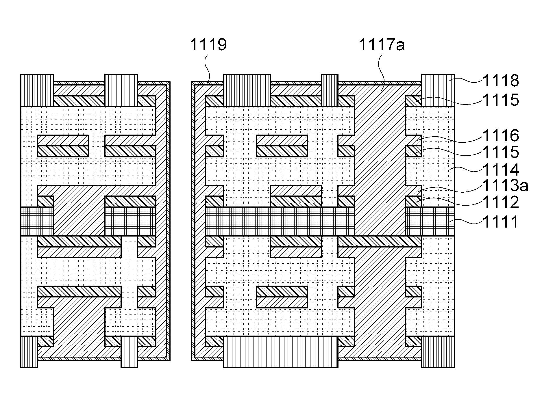
[0031]FIG. 3 is a block diagram roughly showing an embodiment of a method of manufacturing a multilayer PCB in accordance with the present invention, and FIGS. 4a to 4e are configuration diagrams sequentially showing an embodiment of the method of manufacturing a multilayer PCB in accordance with the present invention, wherein FIG. 4a is a configuration diagram roughly showing that a defective inner layer circ...


PUM

PropertyMeasurementUnit
auto optical inspectionaaaaaaaaaa
electrical continuity testaaaaaaaaaa
shapeaaaaaaaaaa

Abstract

The present invention discloses a method of manufacturing a multilayer PCB including: a panel preparation step of preparing a working panel on which a plurality of PCB units having a plurality of inner layer circuit pattern portions are arrayed; a defective portion removing step of removing a defective inner layer circuit pattern portion among the plurality of inner layer circuit pattern portions; a good portion providing step of providing a good inner layer circuit pattern portion in a portion of the working panel, from which the defective inner layer circuit pattern portion is removed; and an outer layer forming step of forming an outer layer circuit pattern portion in the PCB unit. The present invention is capable of improving productivity and reducing manufacturing costs by preventing product loss due to disposal of the PCB unit having the defective inner layer circuit pattern portion.

Description

CROSS-REFERENCE TO RELATED APPLICATIONS[0001]Claim and incorporate by reference domestic priority application and foreign priority application as follows:[0002]CROSS REFERENCE TO RELATED APPLICATION[0003]This application claims the benefit under 35 U.S.C. Section 119 of Korean Patent Application Serial No. 10-2011-0087369, entitled filed Aug. 30, 2011, which is hereby incorporated by reference in its entirety into this application.BACKGROUND OF THE INVENTION[0004]1. Field of the Invention[0005]The present invention relates to a method of manufacturing a multilayer printed circuit board, and more particularly, to a method of manufacturing a multilayer printed circuit board that is capable of reducing manufacturing costs required for disposal at the time of failure of an inner layer circuit pattern portion and improving productivity.[0006]2. Description of the Related Art[0007]In recent times, according to a trend of sets such as a hand-held phone (HHP) and a dye-sensitized solar cell...

Claims


Application Information

Patent Timeline
Patent Type & Authority Applications(United States)
IPC IPC(8): H05K3/02
CPCH05K3/0097H05K3/225Y10T29/49155H05K3/4652Y10T29/49004H05K3/429H05K3/46H05K3/00
Inventor LEE, YANG JEKIM, GI SUKJUNG, JOONG HYUKYANG, DEK GIN
Owner SAMSUNG ELECTRO MECHANICS CO LTD
Why Eureka
Try Eureka