Nitride semiconductor light emitting device and manufacturing method thereof
- Summary
- Abstract
- Description
- Claims
- Application Information
AI Technical Summary
Benefits of technology
Problems solved by technology
Method used
Image

Examples
first embodiment
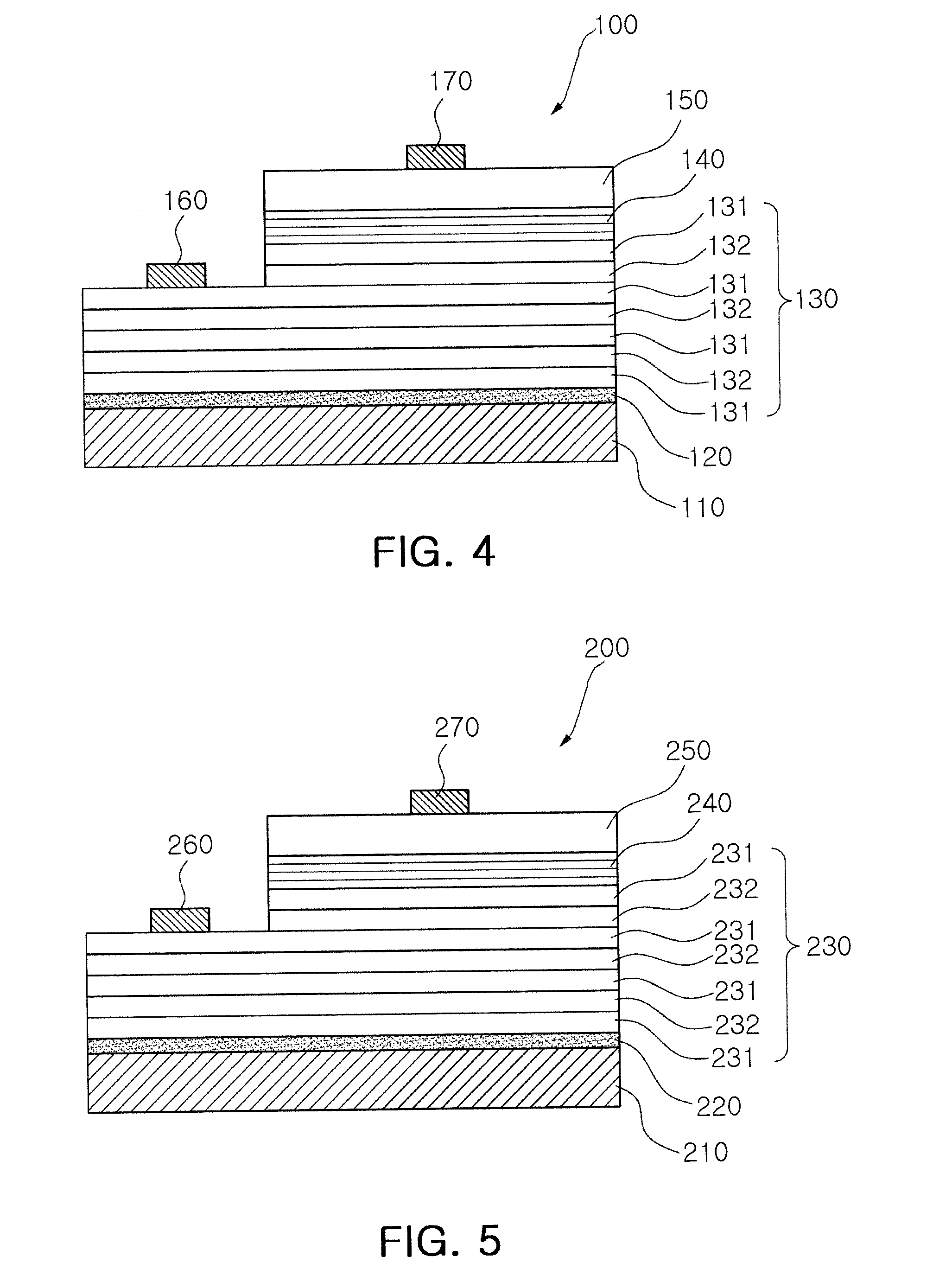
[0029]First, a nitride semiconductor light emitting device 100 according to the present invention and a method for manufacturing the same will be described.
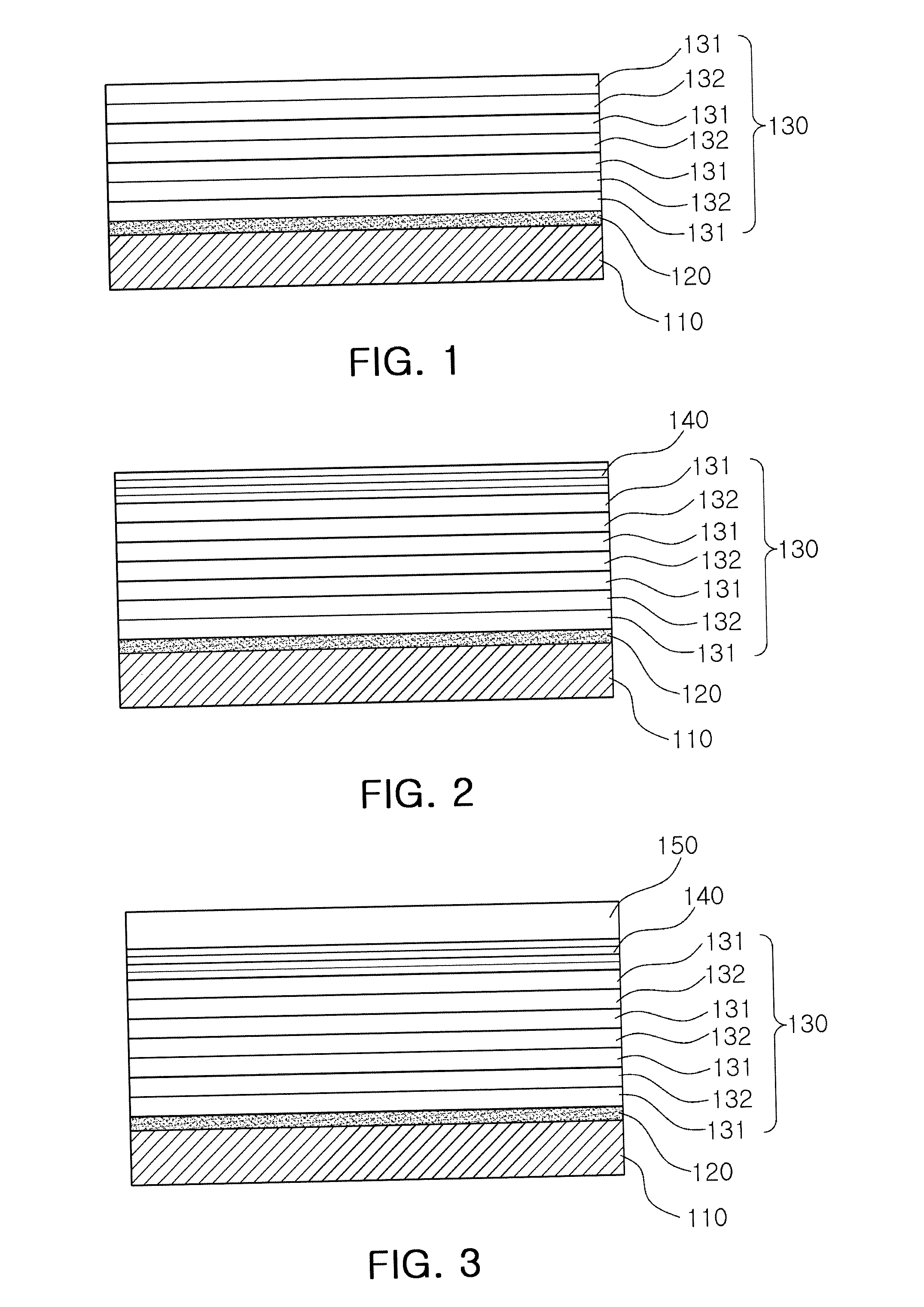
[0030]FIGS. 1 through 4 are cross-sectional views illustrating respective processes of a method for manufacturing a nitride semiconductor light emitting device according to a first embodiment of the present invention.
[0031]A method for manufacturing a nitride semiconductor layer 100 according to a first embodiment of the present invention includes forming a first conductivity-type nitride semiconductor layer 130 including a plurality of indium doped layers 131 on a substrate 110; forming an active layer 140 on the first conductivity-type nitride semiconductor layer 130; and forming a second conductivity-type nitride semiconductor layer 150 on the active layer 140.
[0032]First, as illustrated in FIG. 1, after the substrate 110 is prepared, the first conductivity-type nitride semiconductor layer 130 is formed on the substrate 110.
[0...
second embodiment
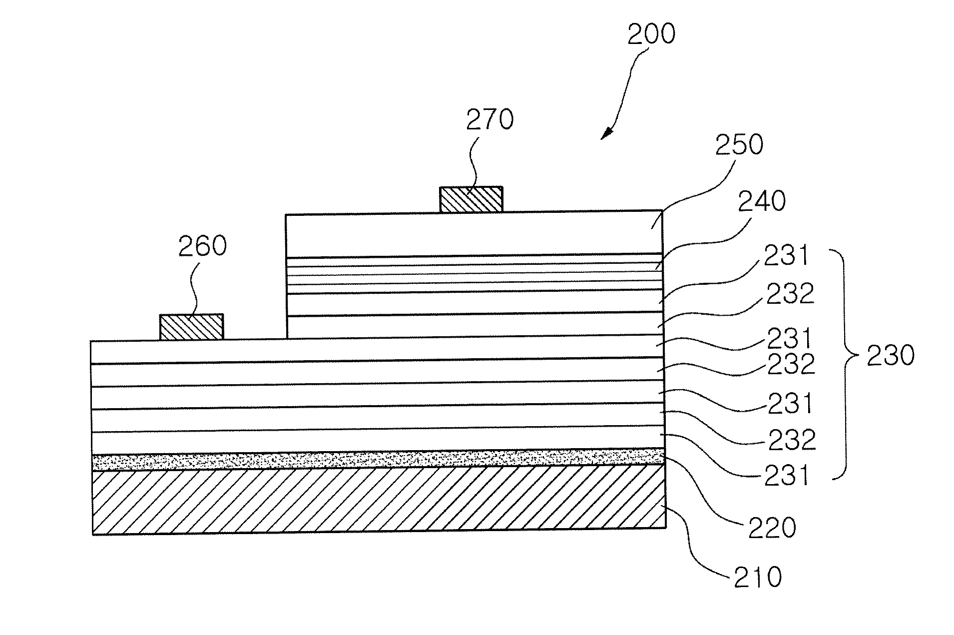
[0050]A nitride semiconductor light emitting device 200 and a manufacturing method thereof according to the present invention will hereinafter be described.
[0051]The nitride semiconductor light emitting device 200 according to the second embodiment of the present invention is manufactured through a similar process to that of the nitride semiconductor light emitting device 100 according to the first embodiment of the present invention, but, unlike the first embodiment as described above, in the second embodiment of the present invention, silicon is co-doped with indium in forming the first conductivity-type nitride semiconductor layer 130.
[0052]First, like the first embodiment as described above, after a substrate 210 is prepared, the first conductivity-type nitride semiconductor layer 230 is formed on the substrate 110. The first conductivity-type nitride semiconductor layer 230 may be made of a semiconductor material having a empirical formula AlxGa(1−x)N, and typically, AlGaN may ...
PUM
 Abstract
Description
Claims
Application Information
 - Generate Ideas
- Intellectual Property
- Life Sciences
- Materials
- Tech Scout
- Unparalleled Data Quality
- Higher Quality Content
- 60% Fewer Hallucinations
Browse by: Latest US Patents, China's latest patents, Technical Efficacy Thesaurus, Application Domain, Technology Topic, Popular Technical Reports.
© 2025 PatSnap. All rights reserved.Legal|Privacy policy|Modern Slavery Act Transparency Statement|Sitemap|About US| Contact US: help@patsnap.com