Solid State Laser Device Using a Selected Crystal Orientation in Non-Polar or Semi-Polar GaN Containing Materials and Methods

a laser device and crystal orientation technology, applied in the field of laser devices, can solve the problems of reducing the efficiency of the device, affecting the performance of the device, and the practical application of the c-plane gan-based laser diodes that have not yet been demonstrated in green or longer wavelengths, so as to facilitate parallel facets and reduce surface roughness

Active Publication Date: 2013-03-14
KYOCERA SLD LASER INC +1
View PDF3 Cites 107 Cited by
  • Summary
  • Abstract
  • Description
  • Claims
  • Application Information

AI Technical Summary

Benefits of technology

[0008]According to the present invention, techniques for manufacture of optical devices are provided. More particularly, the present invention provides a laser device and method using a preferred cleave orientation, which facilitates parallel facets and reduced surface roughness. Although the invention has been described in terms of cleaving, it would be recognized that other ways of forming the facet can be used. As an example, the facets can be etched, cut, separated, split, among others. Additionally, the invention can also be applied to other forms of devices such as light emitting diodes, integrated circuits, MEMS, medical devices, combination of these, among others.
[0017]One or more benefits may be achieved using one or more of the specific embodiments. As an example, the present device and method provides for higher yields over conventional techniques in fabricating facets for laser devices. In other embodiments, the present method and resulting structure are easier to form by way of a preferential cleaving plane in a gallium nitride containing crystalline material. In other embodiments, the present laser device has a pair of facets that are substantially parallel to each other that will provide higher efficiencies, lower optical losses, and reduced threshold currents.

Problems solved by technology

Existing methods suffer from a number of limitations.
Practical c-plane GaN-based laser diodes have not yet been demonstrated in green or longer wavelengths.
A second limitation is that the threshold current of the devices is sometimes undesirably high, which decreases the efficiency of the devices.
A third limitation is that the yield of intact devices tends to be small, mainly due to breakage during the fabrication process.

Method used


Image

  • Solid State Laser Device Using a Selected Crystal Orientation in Non-Polar or Semi-Polar GaN Containing Materials and Methods
  • Solid State Laser Device Using a Selected Crystal Orientation in Non-Polar or Semi-Polar GaN Containing Materials and Methods
  • Solid State Laser Device Using a Selected Crystal Orientation in Non-Polar or Semi-Polar GaN Containing Materials and Methods

Examples


examples

[0052]To prove the principle and operation of the present invention, we performed experiments using GaN substrate materials. In our experiment, we used m-plane GaN crystalline substrates manufactured by Mitsubishi Chemical Corporation, although other commercially available substrates are believed to also work. Details of the present experiments are provided by reference to FIGS. 11 through 12, which are top-view photographs of AFM images of experiment results according to embodiments of the present invention. These photographs are not intended to be limiting. As shown, the photographs illustrate a substantially smooth facet surface, which cleaved preferentially.

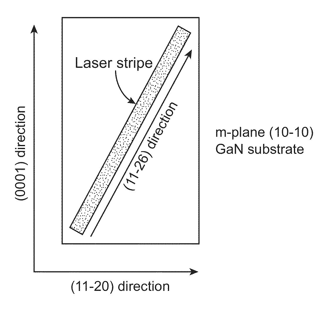
[0053]We discovered a certain plane or planes of a GaN crystalline material that cleaves preferentially to achieve substantially planar faces and desired surface roughness characteristics. In an attempt to prepare a c-plane-oriented cleavage surface on an m-plane, bulk GaN crystal, a series of interrupted laser scribe marks w...


PUM


Abstract

An edge emitting solid state laser and method. The laser comprises at least one AlInGaN active layer on a bulk GaN substrate with a non-polar or semi-polar orientation. The edges of the laser comprise {1 1−2±6} facets. The laser has high gain, low threshold currents, capability for extended operation at high current densities, and can be manufactured with improved yield. The laser is useful for optical data storage, projection displays, and as a source for general illumination.

Description

CROSS-REFERENCES TO RELATED APPLICATIONS[0001]This application is a continuation of U.S. application Ser. No. 12 / 534,838 filed on Aug. 3, 3009, now allowed, which claims priority to U.S. provisional Application No. 61 / 086,142 filed on Aug. 4, 2008, each of which is incorporated by reference herein.BACKGROUND OF THE INVENTION[0002]The present invention relates generally to manufacture of optical devices. More particularly, the present invention provides a laser device and method using a preferred cleave orientation, which facilitates parallel facets and reduced surface roughness. Although the invention has been described in terms of cleaving, it would be recognized that other ways of forming the facet can be used. As an example, the facets can be etched, cut, separated, split, among others. Additionally, the invention can also be applied to other forms of devices such as light emitting diodes, integrated circuits, MEMS, medical devices, combination of these, among others.[0003]Human ...

Claims


Application Information

Patent Timeline
Patent Type & Authority Applications(United States)
IPC IPC(8): H01L21/02H01S5/34H01L29/04H01L29/201H01L29/161H01L29/22
CPCH01S5/0202H01S5/1082H01S5/1085B82Y20/00H01S5/3202H01S5/34333H01S5/2201H01S5/320275H01S5/32025
Inventor SHARMA, RAJATHALL, ERIC M.POBLENZ, CHRISTIANED'EVELYN, MARK P.
Owner KYOCERA SLD LASER INC
Why Eureka
Try Eureka