
Fabricating method of flexible display and flexible display

a flexible display and manufacturing method technology, applied in the field of display, can solve the problems of increasing the manufacturing cost of the display, deterioration of the device characteristics of the display, and damage to the transistor, and achieve the effect of low manufacturing cost and simple release step

Active Publication Date: 2013-03-21
AU OPTRONICS CORP
View PDF2 Cites 33 Cited by
  • Summary
  • Abstract
  • Description
  • Claims
  • Application Information

AI Technical Summary

Benefits of technology

The invention provides a simple and low-cost method to make a flexible display. The method allows for easy release of the patterned release layer and films from the carrier substrate, resulting in a display that is cost-effective and has good device performance.

Problems solved by technology

However, a laser process not only increases the manufacturing cost of the display, but also damages the transistors in the display and causes the device characteristics of the display to deteriorate.

Method used


Image

  • Fabricating method of flexible display and flexible display
  • Fabricating method of flexible display and flexible display
  • Fabricating method of flexible display and flexible display

Examples


Embodiment Construction

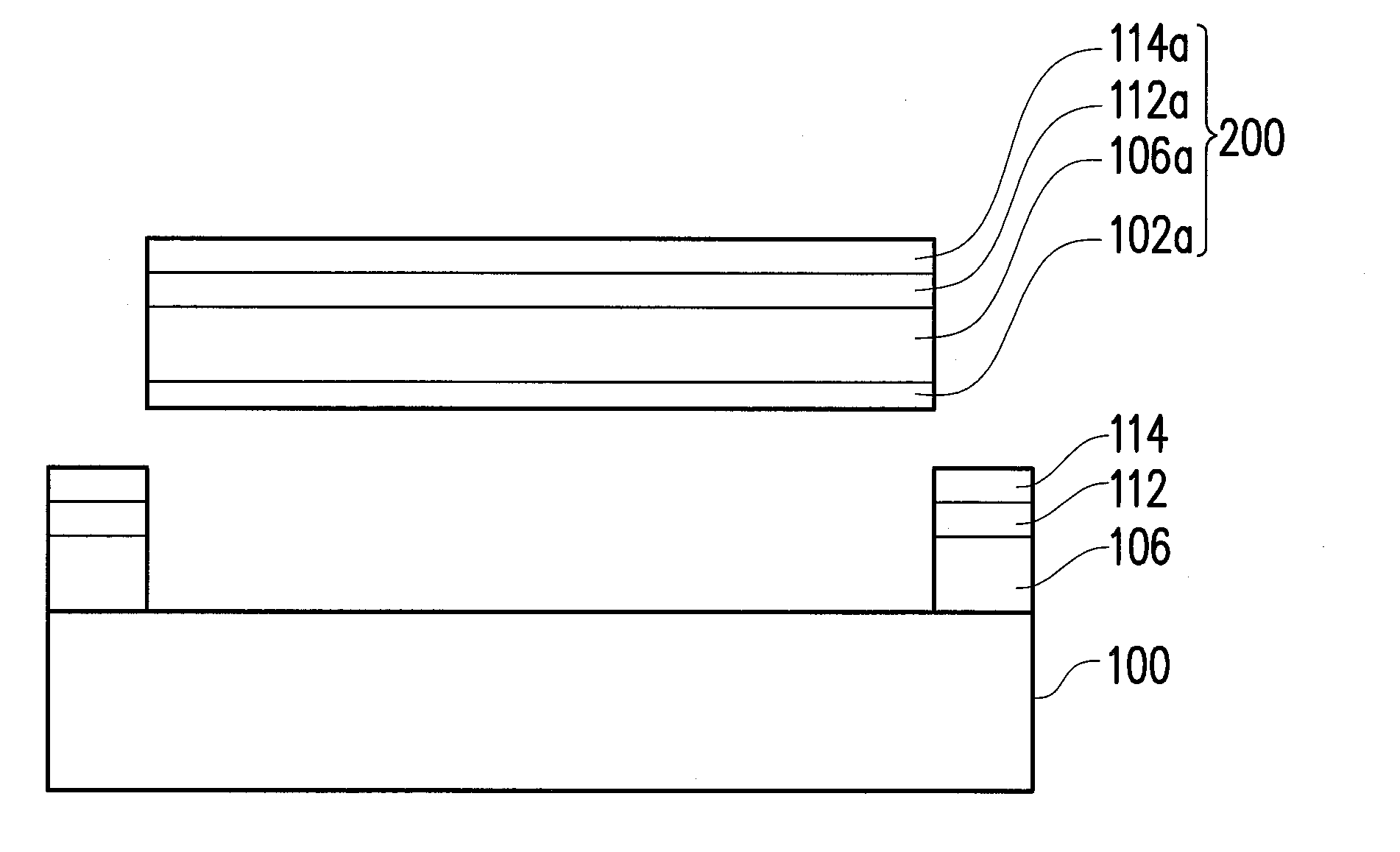
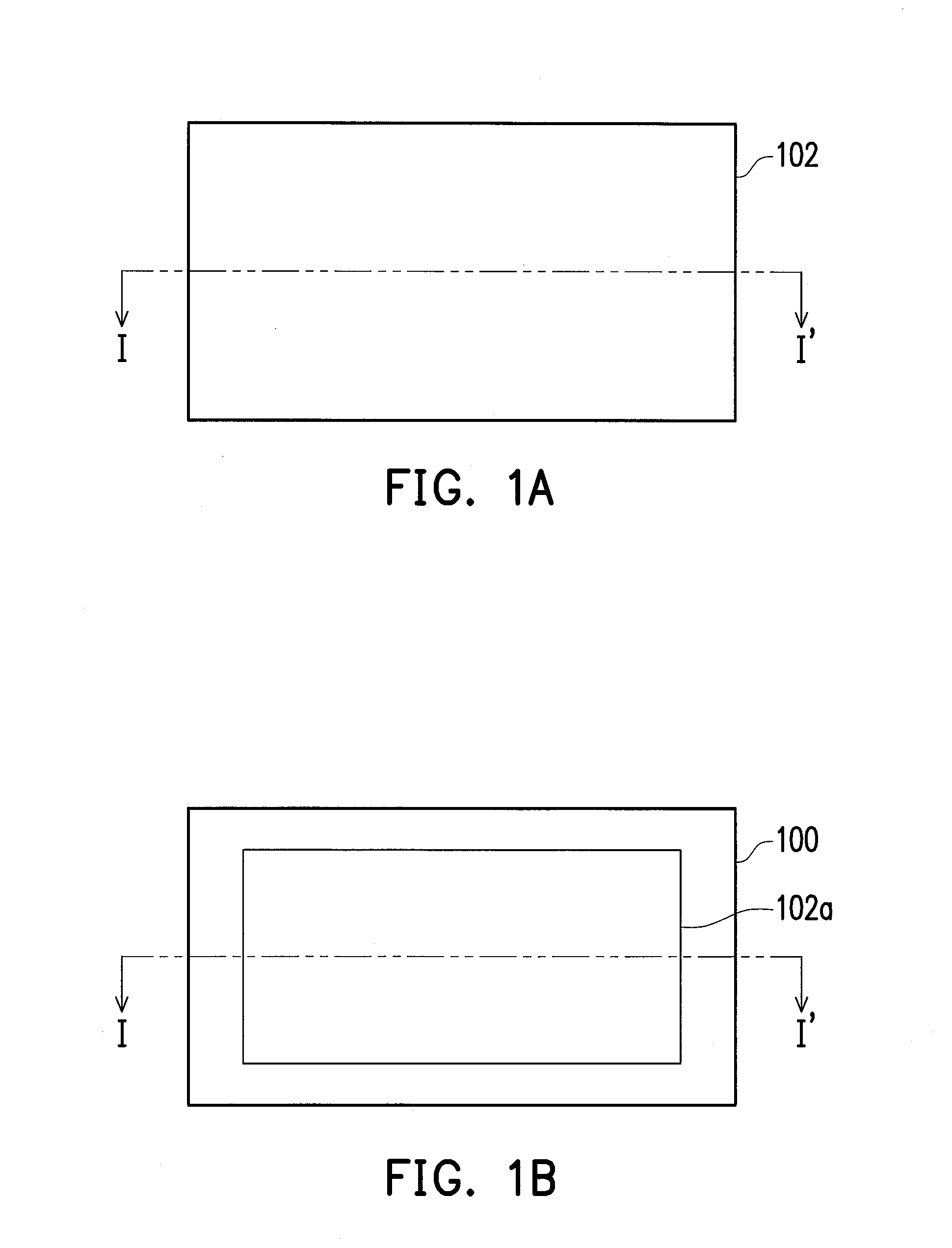
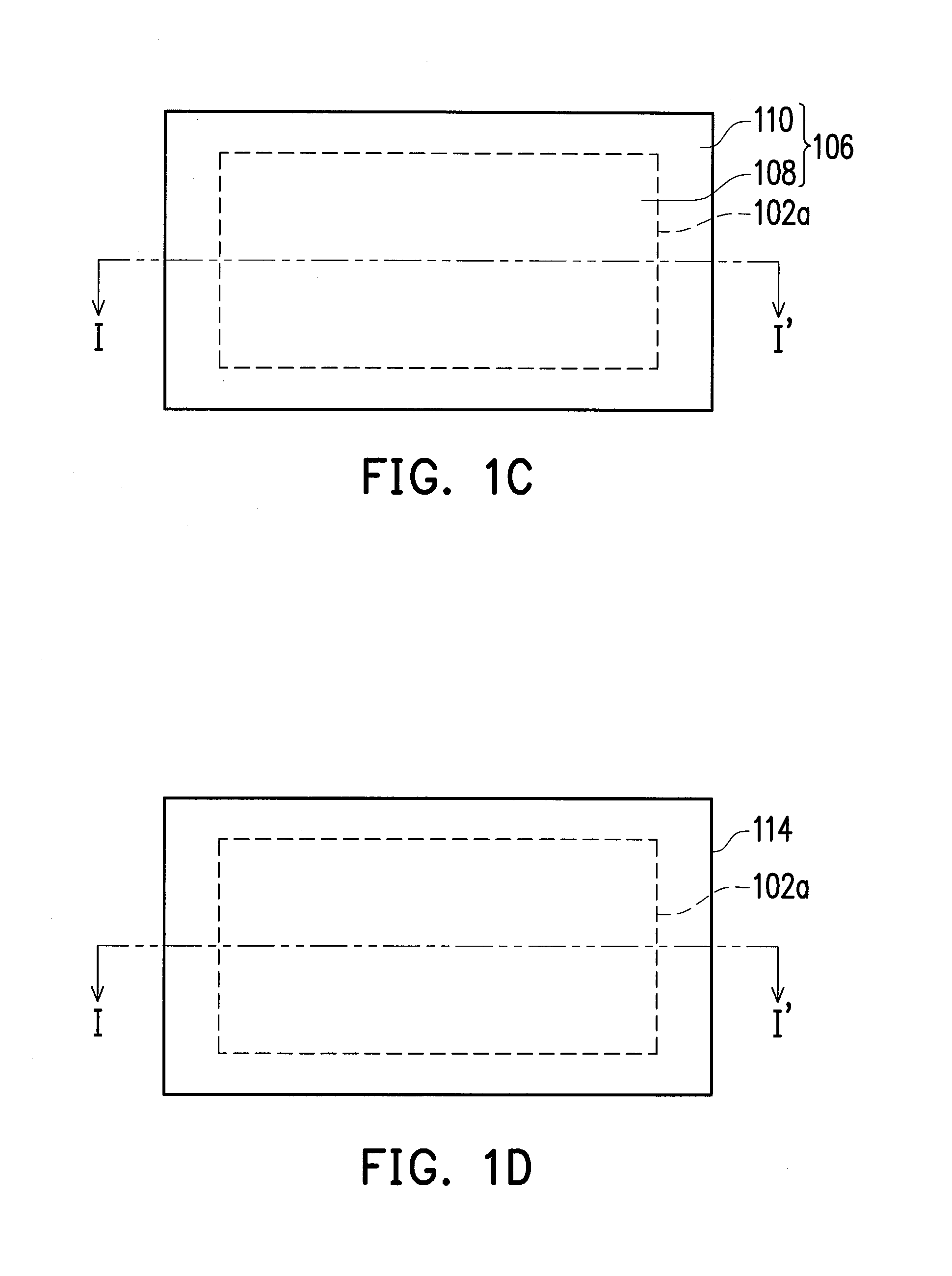
[0017]FIGS. 1A to 1F are schematic top views illustrating a fabricating method of a flexible display according to an embodiment of the invention, and FIGS. 2A to 2F are respective schematic cross-sectional views taken along a line I-I′ line depicted in FIG. 1A to FIG. 1F. Please refer to FIGS. 1A and 2A. First, a release layer 102 is formed on a carrier substrate 100. In the present embodiment, no other films are disposed between the carrier substrate 100 and the release layer 102, for example. The carrier substrate 100 may be a substrate having a high rigidity, a low coefficient of expansion, and a high young's modulus. In the present embodiment, the carrier substrate 100 may be an inorganic substrate, such as a glass substrate. A material of the release layer 102 may be a transparent or an opaque material, such as amorphous silicon. The release layer 102 may be formed by a deposition process such as a chemical vapor deposition (CVD) process, or by other suitable methods, and a pro...


PUM

PropertyMeasurementUnit
Thicknessaaaaaaaaaa
Forceaaaaaaaaaa
Flexibilityaaaaaaaaaa

Abstract

A fabricating method of a flexible display is provided. A release layer is formed on a carrier substrate. The release layer is patterned to form a patterned release layer. A flexible substrate is formed on the patterned release layer, wherein the flexible substrate covers the patterned release layer and a portion of the flexible substrate contacts the carrier substrate. An adhesive force between the patterned release layer and the flexible substrate is larger than an adhesive force between the patterned release layer and the carrier substrate. A device layer is formed on the flexible substrate. A display layer is formed on the device layer. The flexible substrate and patterned release layer are cut simultaneously. The patterned release layer being cut is separated from the carrier substrate, wherein the flexible substrate, the device layer and the display layer which have been cut are sequentially disposed on the separated patterned release layer.

Description

CROSS-REFERENCE TO RELATED APPLICATION[0001]This application claims the priority benefit of Taiwan application serial no. 100133989, filed on Sep. 21, 2011. The entirety of the above-mentioned patent application is hereby incorporated by reference herein and made a part of this specification.BACKGROUND OF THE INVENTION[0002]1. Field of the Invention[0003]The invention relates to a display and a fabricating method thereof. More particularly, the invention relates to a flexible display and a fabricating method thereof.[0004]2. Description of Related Art[0005]With rapid development of display technologies, conventional cathode ray tube (CRT) displays have been gradually replaced by flat panel displays (FPD). In comparison with the FPD formed by a solid carrier (e.g. a glass substrate), a flexible display in which an active device is formed on a flexible substrate has been developed according to recent researches because the flexible substrate (e.g. a plastic substrate) is characterized...

Claims


Application Information

Patent Timeline
IPC IPC(8): B28B7/14B32B27/00
CPCB32B37/26B32B2037/268Y10T428/261G09F9/301B32B2457/20Y10T428/31721
Inventor LIU, CHAN-JUITSAI, CHIH-HUNGFANG, CHUN-HSIANG
Owner AU OPTRONICS CORP
Learn More