Electronic device and image sensor heat dissipation structure

a technology of image sensor and heat dissipation structure, which is applied in the direction of instruments, television systems, and semiconductor/solid-state device details, etc., can solve the problems of image sensor heat dissipation through conduction or convection, and improve the heat dissipation of image sensor with a simple structure, and achieve good heat dissipation effect. , simple structur

Inactive Publication Date: 2013-03-28
ALTEK CORP
View PDF4 Cites 49 Cited by
  • Summary
  • Abstract
  • Description
  • Claims
  • Application Information

AI Technical Summary

Benefits of technology

[0008]The present invention provides an electronic device capable of a good heat dissipation effect through an image sensor heat dissipation structure having a simple structure.
[0009]The present invention provides an image sensor heat dissipation structure adapted to use in an electronic device and capable of a good heat dissipation effect with a simple structure and further improves the efficiency of the electronic device.
[0017]In light of the above, in the electronic device of the present invention, the image sensor can perform heat dissipations through a conduction or convection, since the heat dissipation plate and the thermal interface layer are disposed on the back side of the image sensor. Thus, through the configuration of the image sensor heat dissipation structure, the heat dissipation problem of the electronic device of the present invention can be improved, so that the image sensor can be used with a higher operating frequency and the efficiency of the electronic device is further improved.

Problems solved by technology

However, in such configuration the back surface opposing the light receiving surface of the image sensor is covered by the printed circuit board or flexible printed circuit board, so that the image sensor cannot perform heat dissipation through a conduction or convection.
Thus, in order to make the image sensor meet the development of the portable electronic device market, how to improve the heat dissipation of the image sensor with a simple structure is becoming one of the major issues in the future development.

Method used


Image

  • Electronic device and image sensor heat dissipation structure
  • Electronic device and image sensor heat dissipation structure
  • Electronic device and image sensor heat dissipation structure

Examples


Embodiment Construction

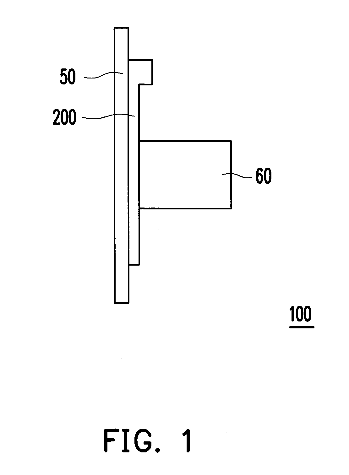
[0023]FIG. 1 is a schematic view of an electronic device according to an embodiment consistent with the invention. Referring to FIG. 1, the electronic device 100 of the embodiment is for example, a camera and includes a main board 50, an image sensor heat dissipation structure 200 and a lens module 60. The image sensor heat dissipation structure 200 is disposed on the main board 50. The lens module 60 is disposed at the image sensor heat dissipation structure 200, and the image sensor heat dissipation structure 200 is located between the lens module 60 and the main board 50.

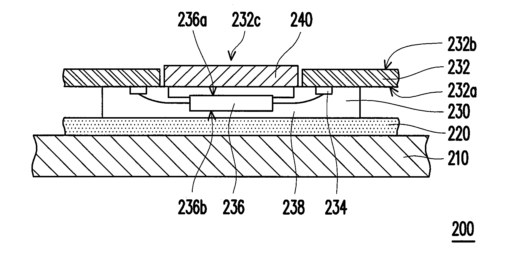
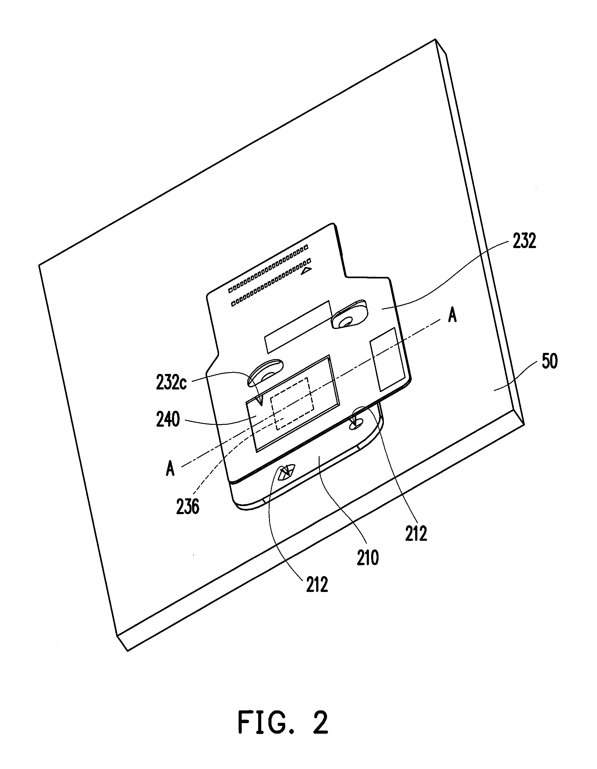
[0024]FIG. 2 is a schematic view of an image sensor heat dissipation structure of the electronic device in FIG. 1. FIG. 3 is a schematic cross-sectional view illustrating the image sensor heat dissipation structure shown in FIG. 2 along the line A-A. Referring to FIG. 2 and FIG. 3 together, the image sensor heat dissipation structure 200 includes a heat dissipation plate 210, a thermal interface layer 220, an ima...


PUM


Abstract

An electronic device including a main board, an image sensor heat dissipation structure and a lens module is provided. The image sensor heat dissipation structure includes a heat dissipation plate, a thermal interface layer, an image sensor package and a cover glass. The heat dissipation plate is fixed to the main board. The thermal interface layer is disposed on the heat dissipation plate. The image sensor package including a circuit board, a plurality of pads, an image sensor and an encapsulant is fixed to the thermal interface layer. The circuit board has an opening. The image sensor is electrically connected to the circuit board through the pads, wherein the light receiving surface faces the opening and the back surface faces the thermal interface layer.

Description

CROSS-REFERENCE TO RELATED APPLICATION[0001]This application claims the priority benefit of Taiwan application serial no. 100134179, filed on Sep. 22, 2011. The entirety of the above-mentioned patent application is hereby incorporated by reference herein and made a part of this specification.BACKGROUND OF THE INVENTION[0002]1. Technical Field[0003]The present invention relates to an electronic device. More particularly, the present invention relates to an electronic device having an image sensor heat dissipation structure.[0004]2. Description of Related Art[0005]Computers, handsets, digital cameras and liquid crystal displays (LCD) are indispensable in the modern people life, but none of them is a product not related to the semiconductor industry. In terms of the peripheral products related to the semiconductor industry, the products are more numerous and various, which demonstrates the solid potential and signification importance of the electronic industry. In recent years, along w...

Claims


Application Information

Patent Timeline
Patent Type & Authority Applications(United States)
IPC IPC(8): H05K7/20
CPCG06F1/20H01L23/36H04N5/2253H01L2924/0002H01L2924/00H04N23/54
Inventor TSAI, YI-YUAN
Owner ALTEK CORP
Why Eureka
Try Eureka