Three-dimensional electronics packaging

a three-dimensional, electronics technology, applied in the direction of electrical apparatus construction details, stacked pcbs, stacked spaced pcbs, etc., can solve the problems of high cost, complexity, and increased complexity of complex solutions, and achieve the effect of improving the quality of the produ

Inactive Publication Date: 2013-04-04
SIERRA WIRELESS
View PDF9 Cites 8 Cited by
  • Summary
  • Abstract
  • Description
  • Claims
  • Application Information

AI Technical Summary

Benefits of technology

[0008]An object of the present invention is to provide three-dimensional electronics packaging. In accordance with an aspect of the present invention, there is provided a printed circuit module (PCM) comprising a printed circuit board (PCB), the PCM defining at least one cavity and configured for operative coupling with an adjacent PCM in a stacked arrangement, wherein the at least one cavity is configured to at least partially accommodate one or more electronic components, the electronic components operatively mounted either on the PCB or on a PCB of the adjacent PCM.
[0009]In accordance with another aspect of the present invention, there is provided a system of two or more printed circuit modules (PCMs) configured for coupling in a stacked arrangement, at least one of the PCMs comprising a printed circuit board (PCB), the PCM defining at least one cavity and configured for operative coupling with an adjacent PCM in a stacked arrangement, wherein the at least one cavity is configured to at least partially accommodate one or more electronic components, the electronic components operatively mounted either on the PCB or on a PCB of the adjacent PCM.
[0010]In accordance with another aspect of the present invention, there is provided a printed circuit assembly (PCA) comprising: a printed circuit board (PCB); a set of one or more components mounted to a side of the PCB; an encapsulant conformally provided over the PCB and the set of one or more components; and one or more channels formed through the encapsulant, each of the one or more channels configured to oper

Problems solved by technology

The continuing trend of densifying electronics systems has led to a variety of design challenges.
This approach offers higher densities than are achievable with traditional two-dimensional printed-circuit board layouts, but at the cost of increased complexity.
Although several solutions to three-dimensional arrangeme

Method used


Image

  • Three-dimensional electronics packaging
  • Three-dimensional electronics packaging
  • Three-dimensional electronics packaging

Examples


Embodiment Construction

Definitions

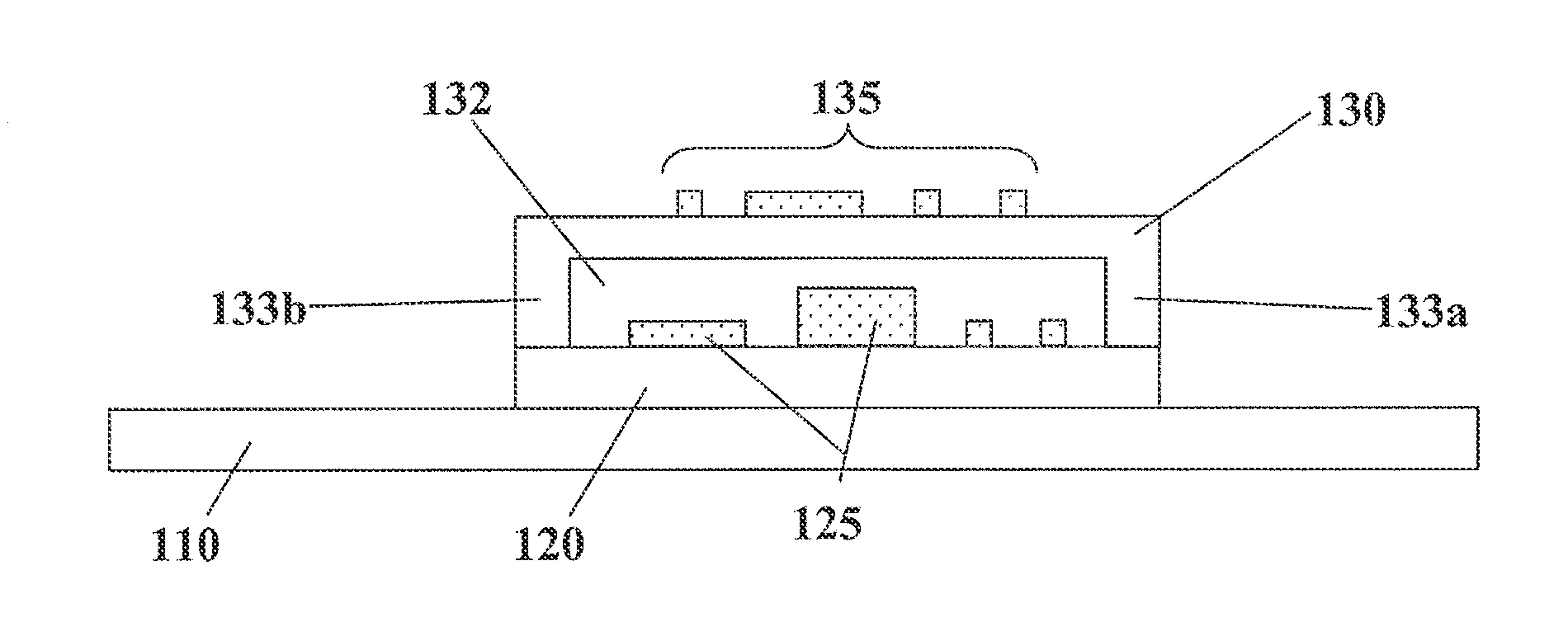
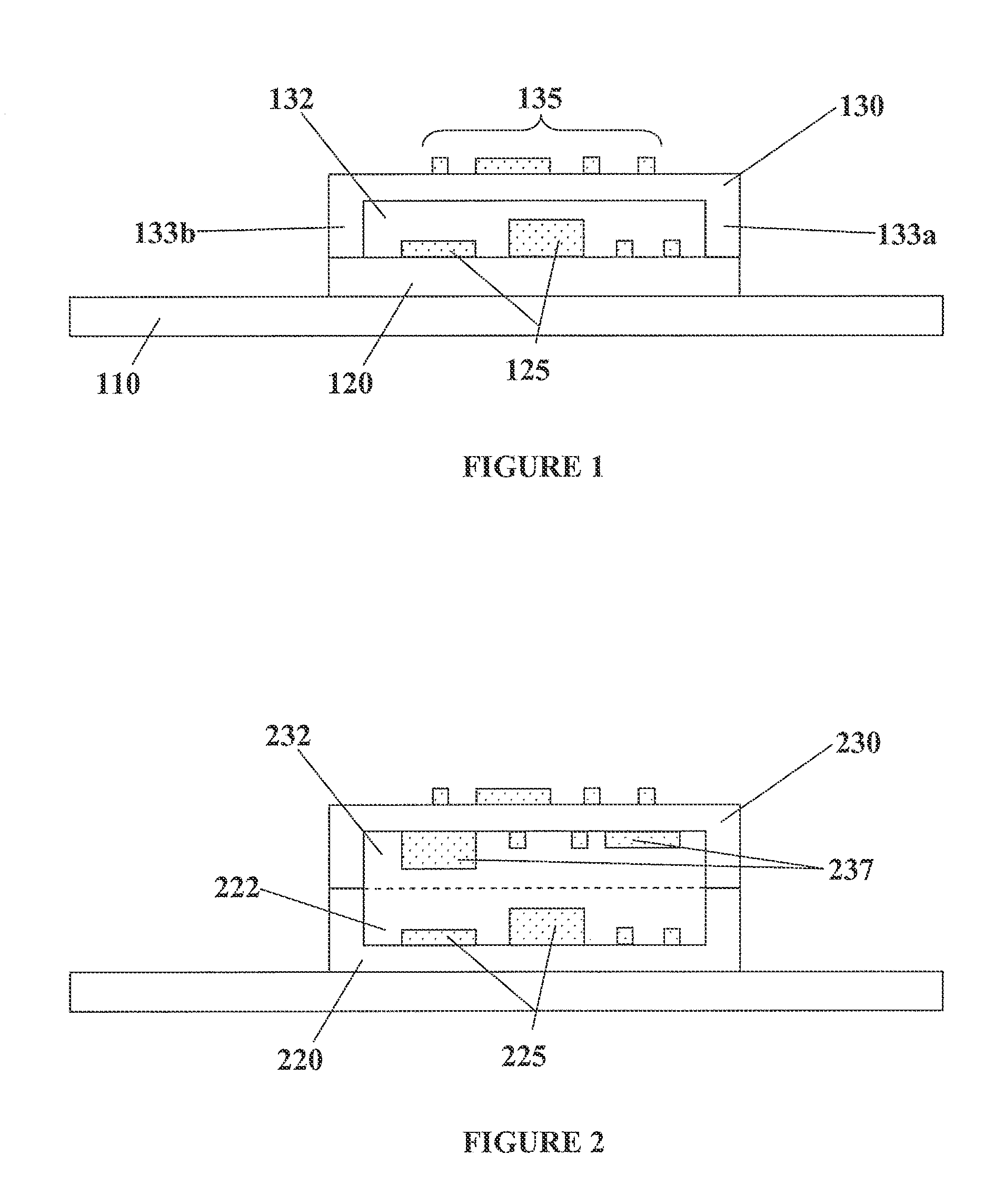
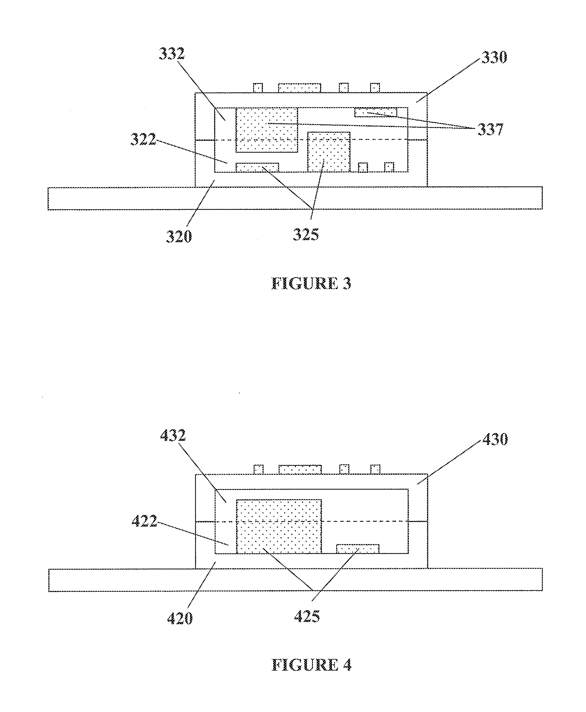
[0029]The term “Printed Circuit Board” or “PCB” refers to a single-sided, double-sided, or multilayer printed circuit board to which components may be attached, for example by soldering.

[0030]The term “Printed Circuit Assembly” or “PCA” refers to a PCB along with electronics components, such as chips, and / or other structural components such as frames or spacers attached thereto.

[0031]The term “Printed Circuit Module” or “PCM” is used generically to refer to either a PCB or a PCA. A PCM may or may not include an encapsulant.

[0032]The term “Chip” refers to a packaged electronic device, such as a semiconductor device, integrated circuit, set of semiconductor devices or integrated circuits, or the like. The package may be a plastic chip carrier, ceramic chip carrier, or other suitable package. The package typically comprises one or more electrical connectors such as pins, pads, leads, apertures, vias, solder balls, solder bumps, or the like, operatively coupled to the electro...


PUM


Abstract

Solutions for providing stackable electronics packaging are provided. In some embodiments, electronic components are accommodated in the cavity of a printed circuit board (PCB) or printed circuit assembly (PCA), or co-accommodated in adjoining cavities of adjacent, stacked PCAs or PCBs. The cavities allow for closer stacking of the PCAs or PCBs. In some embodiments, a PCA comprises an encapsulant conformally layered over a PCB with electronic components mounted on top and bottom. Power and/or signal channels are routed through the encapsulant to the top and/or bottom layers. The encapsulated PCAs may be stacked. In various embodiments, stackable PCAs are modular, facilitating customization.

Description

FIELD OF THE INVENTION[0001]The present invention pertains in general to electronics packaging and in particular to aspects of three-dimensional electronics packaging.BACKGROUND[0002]The continuing trend of densifying electronics systems has led to a variety of design challenges. Increased density can have significant benefits, such as increased system speed and efficiency, improved signal synchronization, decreased size, and improved portability. To achieve greater electronics densities, some designers have turned to arranging and interconnecting electronics components in three dimensions. This approach offers higher densities than are achievable with traditional two-dimensional printed-circuit board layouts, but at the cost of increased complexity.[0003]Example approaches to three-dimensional arrangements of electronics components are Stacked System in Package (SiP) technology (for example Chip-stack Multi-chip Modules) and Package on Package (PoP) technology. Stacked SiPs include...

Claims


Application Information

Patent Timeline
IPC IPC(8): H05K7/00
CPCH05K1/141H05K1/144H05K3/284H05K3/4697H05K2201/041H05K2201/042H01L2924/0002H05K2201/047H01L23/13H01L2924/00
Inventor SYAL, ASHISHSAMUELS, BRUCE RICHARD JOHNPOURSEYED, BEHROUZMYTTING, CHRISSCHERPEREEL, AUDREYNEWMAN, PAUL
Owner SIERRA WIRELESS
Why Eureka
Try Eureka