Semiconductor chip package including voltage generation circuit with reduced power noise

a technology of a semiconductor chip and a power noise reduction, applied in the direction of semiconductor/solid-state device details, digital storage, instruments, etc., can solve the problems of weak ivc to power noise, the level of an external voltage applied through an external voltage supply terminal may be changed, and the difficulty in freely changing a level of external voltage when necessary, so as to and reduce the level of distortion and interference

Active Publication Date: 2013-04-11
SAMSUNG ELECTRONICS CO LTD
View PDF5 Cites 4 Cited by
  • Summary
  • Abstract
  • Description
  • Claims
  • Application Information

AI Technical Summary

Benefits of technology

[0009]The present general inventive concept provides a semiconductor chip package to reduce power noise in a circuit when it receives a supply voltage from an external source to provide voltage for an internal circuit. Embodiments of the present general inventive concept provide a semiconductor chip package including: an integrated circuit chip that includes a voltage generation circuit that receives an external voltage to generate a supply voltage to be used in an internal circuit and a connection terminal connected to an output node of the voltage generation circuit; and a mounting substrate that includes a noise eliminator electrically connected to the connection terminal to reduce power noise of the supply voltage and mount the integrated circuit chip to package the integrated circuit chip as the semiconductor chip package.
[0011]The foregoing and / or other features and utilities of the inventive concept can substantially be achieved by providing a semiconductor chip package including: an integrated circuit chip including an external voltage supply circuit that receives an external voltage to distribute: a voltage generation circuit that receives the external voltage distributed by the external voltage supply circuit to generate a supply voltage to be used in an internal circuit: a first connection terminal connected to an input node of the external voltage supply circuit and a second connection terminal connected to an output terminal of the supply voltage of the voltage generation circuit; and a mounting substrate including a first and a second noise eliminator independently connected to the first and second terminals to reduce a power noise of the external voltage and the supply voltage and to mount the integrated circuit chip to package the integrated circuit chip as the semiconductor chip package.
[0012]The foregoing and / or other features and utilities of the inventive concept can substantially be achieved by providing by an electronic apparatus including an interface unit to receive an external voltage from an external supply source, a semiconductor chip package that may include an integrated circuit chip including a voltage generation circuit that receives the external voltage from the external supply source to generate a supply voltage to be used in an internal circuit and a connection terminal connected to an output node of the voltage generation circuit, and a mounting substrate including a noise eliminator electrically connected to the connection terminal to reduce a power noise of the supply voltage and to mount the integrated circuit chip to package the integrated circuit chip as the semiconductor package, and a control unit to control the semiconductor chip package to process a function of the electronic apparatus to be associated with data of the semiconductor chip package.
[0013]The noise eliminator may be formed outside of the integrated circuit chip and may reduce a power noise of the external voltage supplied from the external supply source.
[0015]The noise eliminator may allow the input unit to input the user command with a reduced level of distortion and interference and the interface unit to receive the audio and video image data with a reduced level of distortion and interference from the external device.
[0016]The electronic apparatus may further include a functional unit to process the input command and the audio and video image data and the control unit can control a display unit to display the audio and video image data with the reduced level of distortion and interference.

Problems solved by technology

A level of an external voltage applied through an external voltage supply terminal may be changed by an external environment or a power noise generated when an integrated circuit chip operates.
However, it is difficult to change a level of external voltage freely when necessary.
However, the IVC is weak to power noise caused by a speed up of an internal circuit connected to a voltage generation circuit.

Method used


Image

  • Semiconductor chip package including voltage generation circuit with reduced power noise
  • Semiconductor chip package including voltage generation circuit with reduced power noise
  • Semiconductor chip package including voltage generation circuit with reduced power noise

Examples


Embodiment Construction

[0029]Embodiments of present general inventive concept will be described more fully hereinafter with reference to the accompanying drawings, in which embodiments of the invention are shown. This present general inventive concept may, however, be embodied in many different forms and should not be construed as limited to the embodiments set forth herein. Rather, these embodiments are provided so that this disclosure will be thorough and complete, and will fully convey the scope of the present general inventive concept to those skilled in the art. In the drawings, the size and relative sizes of layers and regions may be exaggerated for clarity. Like numbers refer to like elements throughout.

[0030]It will be understood that when an element is referred to as being “connected” or “coupled” to another element, it can be directly connected or coupled to the other element or intervening elements may be present.

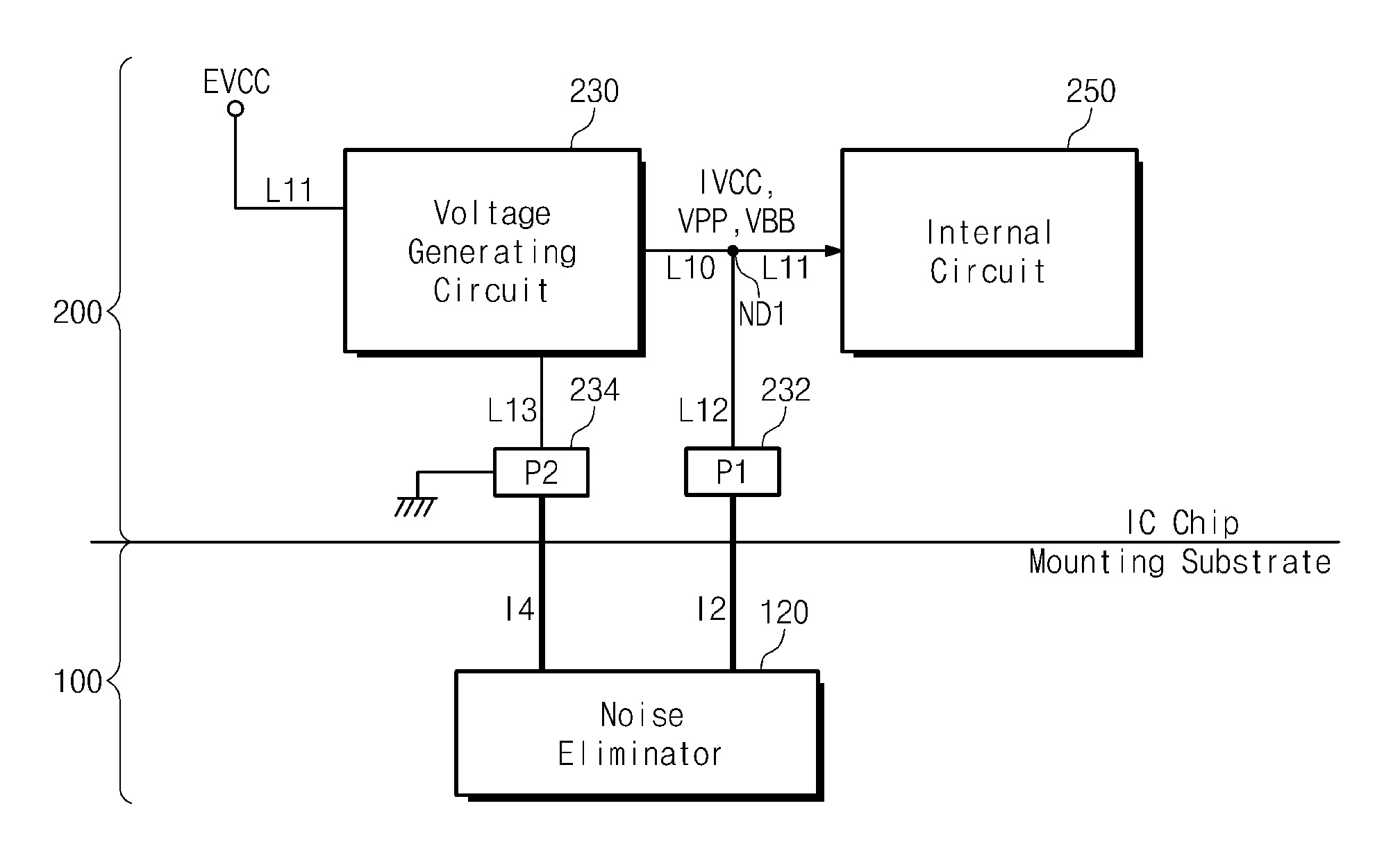
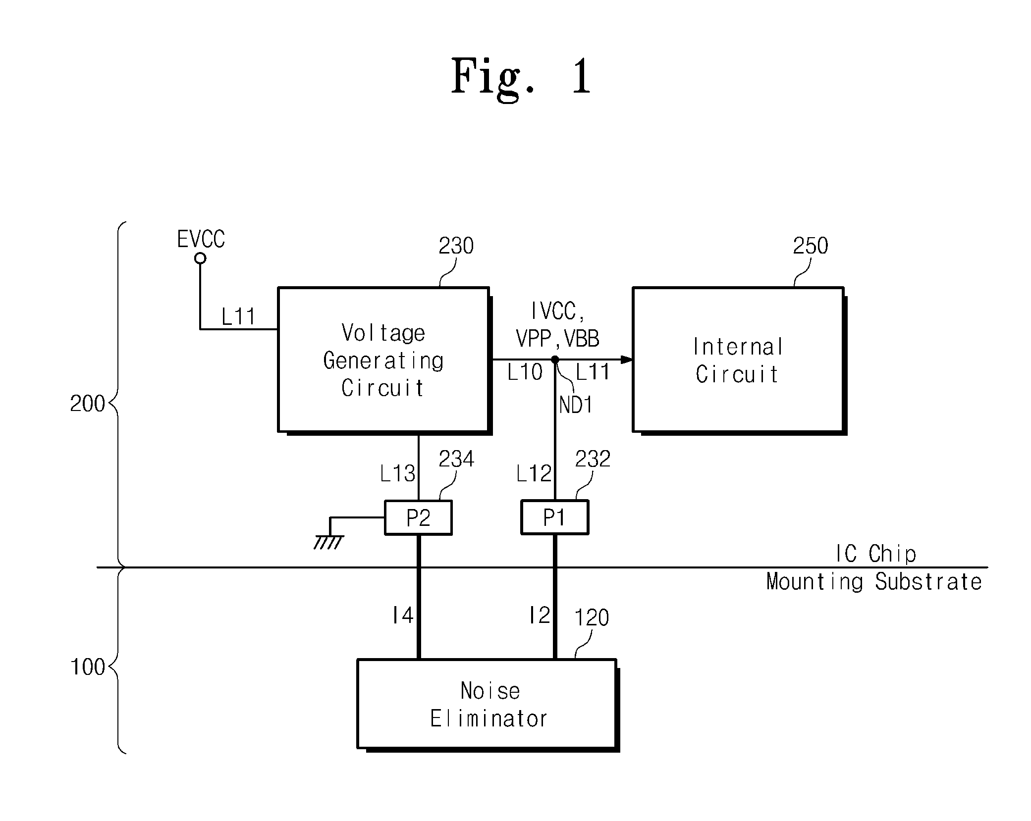
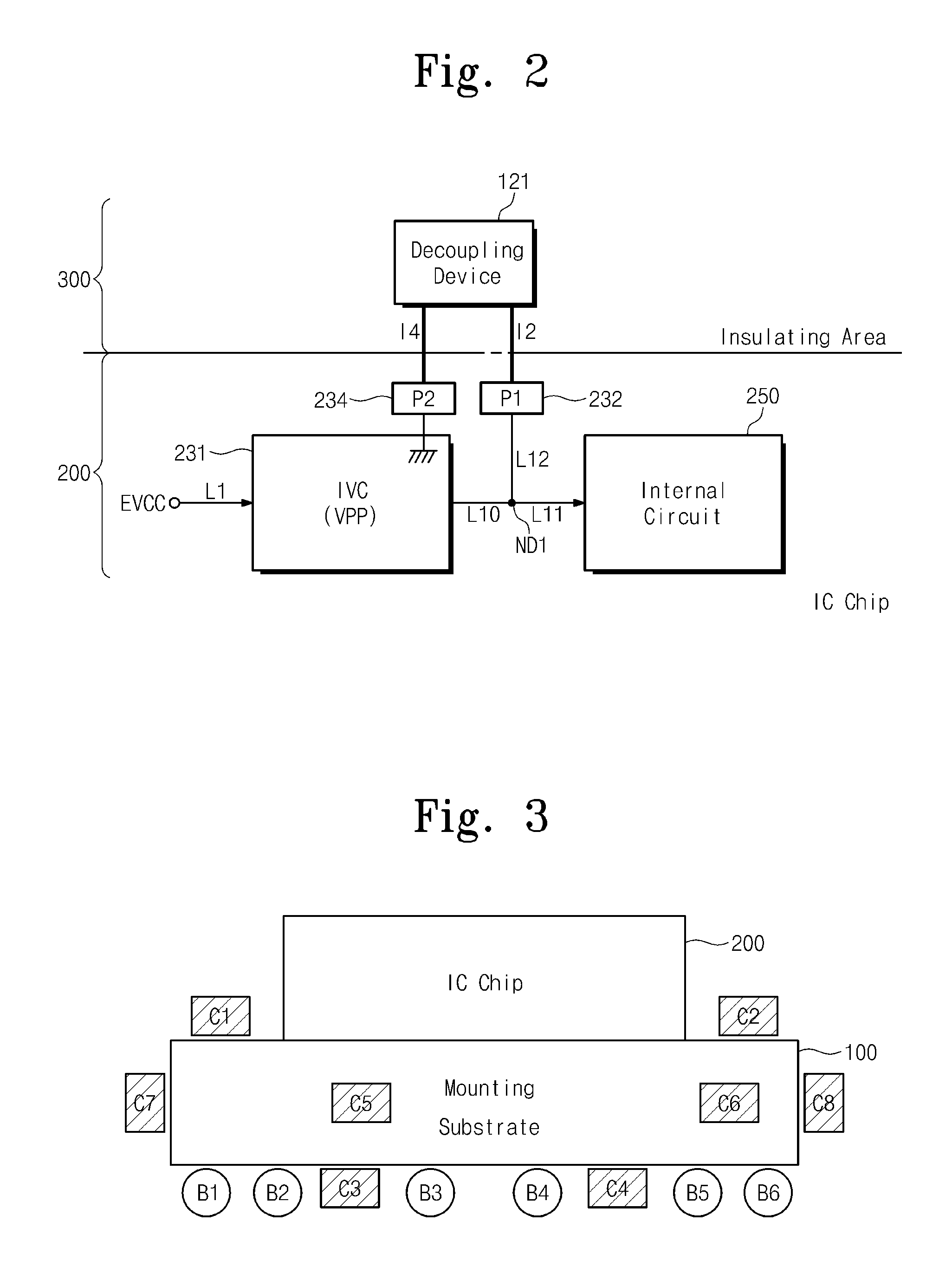
[0031]FIG. 1 is a circuit connection diagram of a semiconductor chip package accor...


PUM


Abstract

A semiconductor chip package illuminates and minimizes a power noise generated from a voltage generation circuit in the semiconductor chip package includes an integrated circuit chip with a voltage generation circuit that receives an external voltage to generate a supply voltage to be used in an internal circuit and a connection terminal connected to an output node of the voltage generation circuit, and a mounting substrate including a noise eliminator electrically connected to the connection terminal to reduce a power noise of the supply voltage and a mounting substrate to mount the integrated circuit chip to package the integrated circuit chip as the semiconductor chip package.

Description

CROSS-REFERENCE TO RELATED APPLICATIONS[0001]This U.S. non-provisional patent application claims priority under 35 U.S.C. §119 of Korean Patent Application No. 10-2011-0103018, filed on Oct. 10, 2011, the entire contents of which are hereby incorporated by reference.BACKGROUND[0002]1. Field[0003]The present general inventive concept herein relates to an apparatus to remove power noise in an integrated circuit chip, and more particularly, to a semiconductor chip package to reduce power noise in a circuit which receives an external supply voltage to provide a supply voltage for an internal circuit.[0004]2. Description of the Related Art[0005]An integrated circuit chip including a semiconductor memory such as a dynamic random access memory (hereinafter DRAM) operates by receiving a power supply from an outside power source thereof after being packaged. A level of an external voltage applied through an external voltage supply terminal may be changed by an external environment or a power...

Claims


Application Information

Patent Timeline
Patent Type & Authority Applications(United States)
IPC IPC(8): H01L25/00
CPCH01L23/642G11C11/4074H01L2924/0002H01L2924/00G11C5/14H01L23/58
Inventor KANG, SUNWONKIM, CHIWOOKWOO, HYUN JEONGHWANG, SANGJOON
Owner SAMSUNG ELECTRONICS CO LTD
Why Eureka
Try Eureka