Semiconductor device performing burst order control and data bus inversion

a technology of data bus and semiconductor device, applied in the field of semiconductor device, can solve the problems of high power consumption and need for a reduction of boc circui

Active Publication Date: 2013-04-11
LONGITUDE LICENSING LTD
View PDF7 Cites 12 Cited by
  • Summary
  • Abstract
  • Description
  • Claims
  • Application Information

AI Technical Summary

Benefits of technology

[0011]In still another embodiment, there is provided a device that includes: a burst order control circuit configured to receive a first data signal and then a second data signal, each of the first and second data signals including a plurality of bits, and output the second data signal and then the first data signal based on a control signal; and an inversion control circuit configured to receive the second data signal and then the first data signal and output the second data signal and then the first data signal, the bits of one of the second and first data signals being non-inverted based on a first information and the bits of the other of the bits of the second and first data signal being inverted based on a second information, the first and second information being obtained from the respective bits of the second and first data signals, the first and second information being output from the inversion control circuit.

Problems solved by technology

Also, the higher power consumption also needs a reduction of the BOC circuits.

Method used


Image

  • Semiconductor device performing burst order control and data bus inversion
  • Semiconductor device performing burst order control and data bus inversion
  • Semiconductor device performing burst order control and data bus inversion

Examples


Embodiment Construction

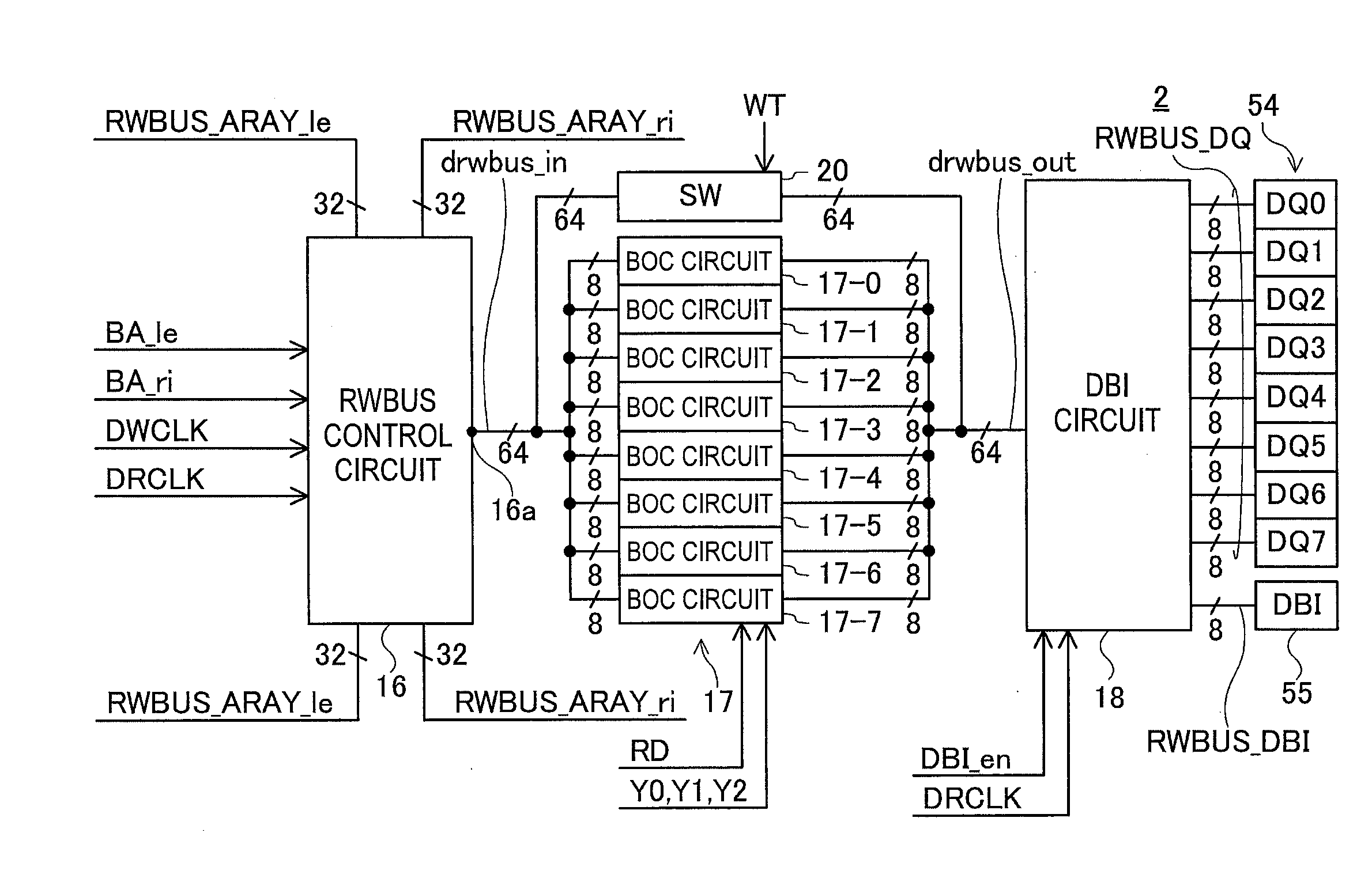
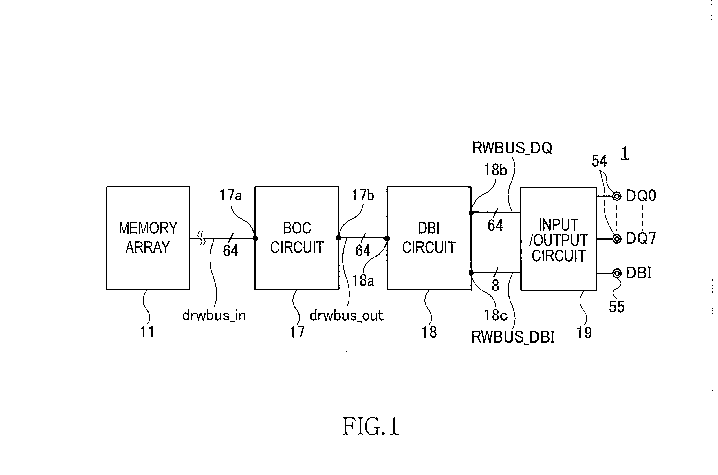
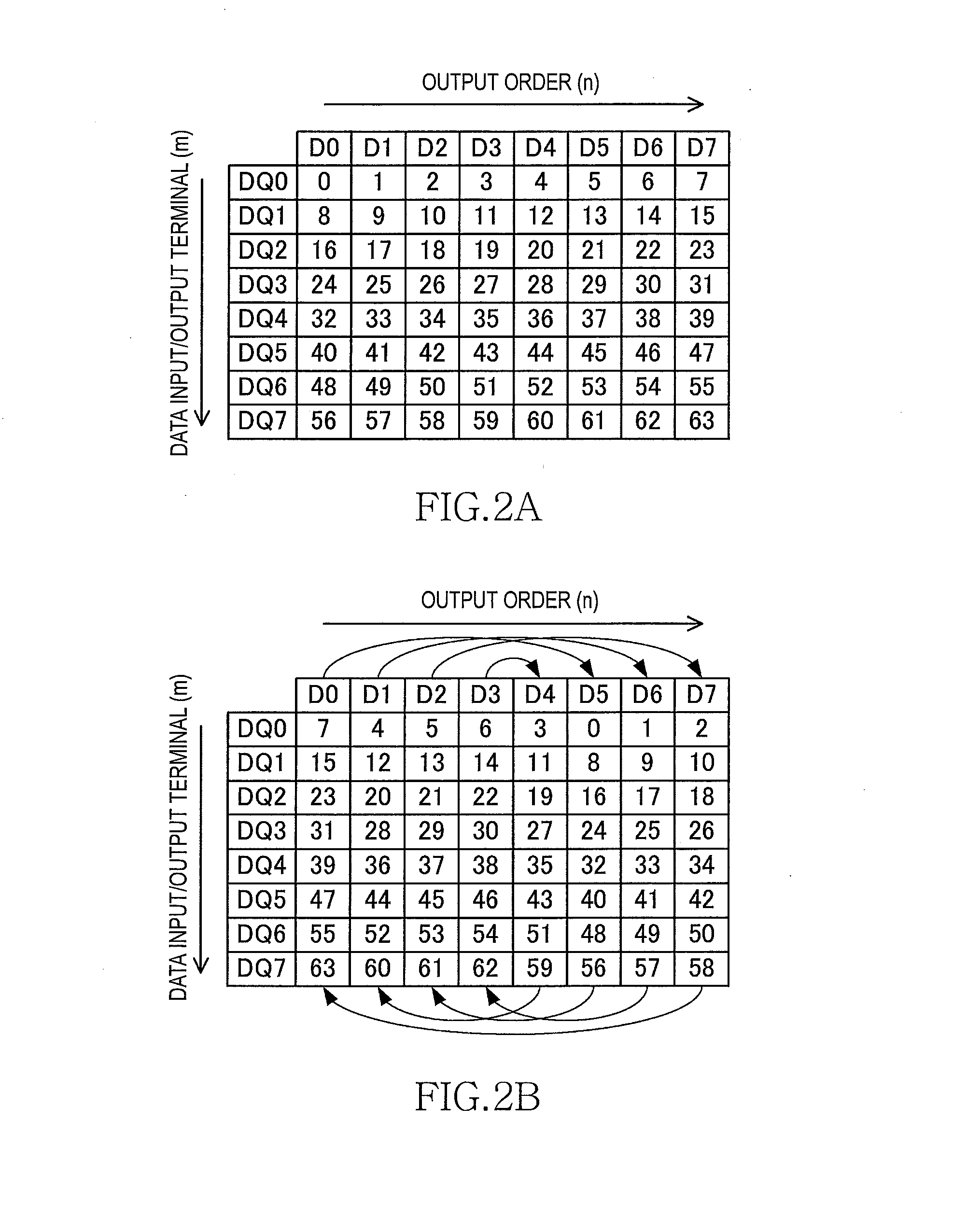
[0028]An embodiment of the present invention will be described below. It will be understood that what the present invention claims are not limited to such an embodiment. Specifically, a semiconductor device according to the embodiment of the present invention includes: a plurality of first data lines (drwbus_in) that transmit a plurality of sequential (ordered) first data bits (64 bits of read data prefetched from a memory cell), respectively; a plurality of second data lines (drwbus_out) that transmit a plurality of sequential second data bits, respectively; a plurality of third data lines (RWBUS_DQ) that transmit a plurality of sequential third data bits, respectively; and a plurality of fourth data lines (RWBUS_DBI) that transmit a plurality of sequential fourth data bits, respectively. The semiconductor device according to the embodiment of the present invention further includes: a BOC circuit that rearranges order of the plurality of first data bits (read data DQ) supplied from...


PUM


Abstract

Disclosed herein is a device that a device including first data lines transmitting a plurality of sequential first data bits, respectively, second data lines transmitting a plurality of sequential second data bits, respectively, third data lines transmitting a plurality of sequential third data bits, respectively, a BOC circuit rearranging order of the plurality of first data bits supplied from the plurality of first data lines in accordance with address information, the BOC circuit supplying the resultant to the plurality of second data lines as the plurality of second data bits, and a DBI circuit performing inversion or non-inversion of the plurality of second data bits supplied from the plurality of second data lines independently of each other in accordance with a predetermined condition, the DBI circuit supplying the resultant to the plurality of third data lines as the plurality of third data bits.

Description

BACKGROUND OF THE INVENTION[0001]1. Field of the Invention[0002]The present invention relates to a semiconductor device, and more particularly to a semiconductor device that performs burst order control (BOC) and data bus inversion (DBI). The present invention also relates to a data processing system including such a semiconductor device.[0003]2. Description of Related Art[0004]DDR3, the dominant standard of dynamic random access memory (DRAM), and the next-generation standard DDR4 use a technology called BOC for suitable random access. For example, by BOC with a burst length of eight, the output order of eight bits of read data to be consecutively output from a data input / output terminal is rearranged according to three bits of column address Y0, Y1, and Y2 that are input from an external controller. The external controller can thus take out the pieces of data stored in memory cells in a desired order. BOC is not applied to write data. Japanese Patent Application Laid-Open No. H06-...

Claims


Application Information

Patent Timeline
Patent Type & Authority Applications(United States)
IPC IPC(8): G06F12/00
CPCG06F12/00G11C7/1006G11C11/4096G11C7/1027G11C7/1012
Inventor SHIDO, TAIHEIDONO, CHIAKIKONDO, CHIKARAMIYAZAKI, SHINYA
Owner LONGITUDE LICENSING LTD
Why Eureka
Try Eureka