Alignment net insertion for straightening the datapath in a force-directed placer

a force-directed placer and datapath technology, applied in the field of semiconductor chips and integrated circuits, can solve the problems of large number of cells, difficult to achieve physical design without the aid of computers, and require complicated connections between cells, so as to reduce overlap and improve efficiency. area usage

Inactive Publication Date: 2013-04-18
GLOBALFOUNDRIES INC
View PDF6 Cites 11 Cited by
  • Summary
  • Abstract
  • Description
  • Claims
  • Application Information

AI Technical Summary

Benefits of technology

[0010]The present invention is generally directed to a method of placing cells in a layout of an integrated circuit design by receiving a circuit description of the integrated circuit design which includes cells interconnected to form true nets, designating a preferred direction for cell alignment in the layout, identifying a set of the cells defining a datapath which is to be aligned along the preferred direction, inserting in the circuit description an artificial alignment net which interconnects all cells in the set, and placing the cells in the layout using a wirelength optimization which assigns weights to wire sections of nets based on the preferred direction. In an example wherein the preferred direction is horizontal, the placer assigns weights to vertical wire sections that are greater than weights assigned to horizontal wire sections. The rate of change of the alignment weighting value preferably increases slowly during the initial stages

Problems solved by technology

An IC may include a very large number of cells and require complicated connections between the cells.
Due to the large number of components and the details required by the fabrication process for very large scale integrated (VLSI) devices, physical design is not practical

Method used


Image

  • Alignment net insertion for straightening the datapath in a force-directed placer
  • Alignment net insertion for straightening the datapath in a force-directed placer
  • Alignment net insertion for straightening the datapath in a force-directed placer

Examples


Embodiment Construction

)

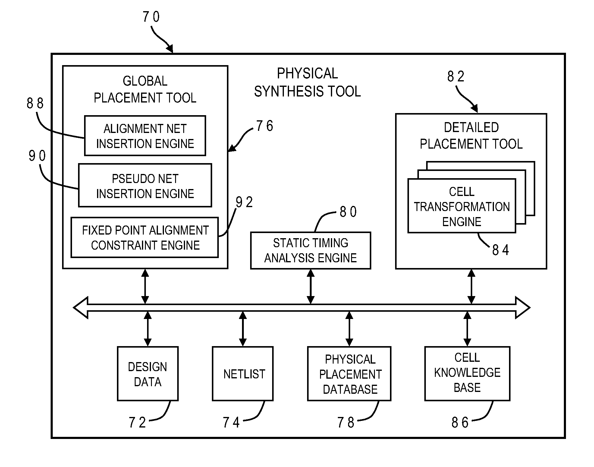
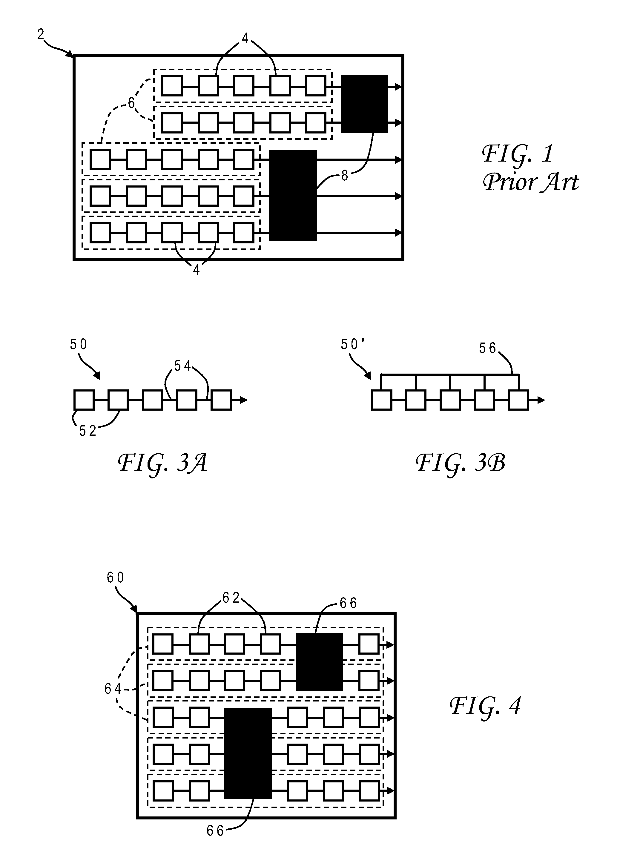
[0021]Current microprocessor trends are integrating traditionally custom designs with random logic macros (RLMs) into very large integrated circuit designs. In some cases, entire microprocessor units are designed using an automated synthesis flow that integrates these traditional custom designs and RLMs. This type of merged synthesis run is referred to as large block synthesis (LBS). The LBS blocks, i.e., sets of cells or logic modules, require handling dataflow designs differently than traditional RLMs. In particular, as the size of the designs grow, there is a need for improved automated datapath design. Conventional placement tools typically result in designs with critical datapaths that zig-zag and criss-cross all over the layout area.

[0022]It would accordingly be desirable to devise an improved placer which could straighten out these datapaths, but with current placement models there is no way to provide a constraint to tell the placer that a datapath should be straight. Weigh...


PUM


Abstract

An automated method for aligning a critical datapath in an integrated circuit design inserts an artificial alignment net in the netlist which interconnects all cells in the bit stack of the datapath. The cells are placed using a wirelength optimization which assigns weights to wire sections based on the alignment direction. The rate of change of the alignment weighting value can vary during different stages of global placement. The invention is particularly suited for a force-directed placer which uses a linear system solver to obtain a globally optimum solution for placement of the cells having some overlap among the cells, and thereafter spreads the cells to reduce the overlap. Pseudo nets are also inserted which interconnect a cell and an expected location of the cell after spreading for that iteration.

Description

BACKGROUND OF THE INVENTION[0001]1. Field of the Invention[0002]The present invention generally relates to the design of semiconductor chips and integrated circuits, and more particularly to a method of placing components of an integrated circuit design in a layout.[0003]2. Description of the Related Art[0004]Integrated circuits are used for a wide variety of electronic applications, from simple devices such as wristwatches, to the most complex computer systems. A microelectronic integrated circuit (IC) chip can generally be thought of as a collection of logic cells with electrical interconnections between the cells, formed on a semiconductor substrate (e.g., silicon). An IC may include a very large number of cells and require complicated connections between the cells. A cell is a group of one or more circuit elements such as transistors, capacitors, resistors, inductors, and other basic circuit elements combined to perform a logic function. Cell types include, for example, core cel...

Claims


Application Information

Patent Timeline
IPC IPC(8): G06F17/50
CPCG06F17/5072G06F30/392G06F30/00
Inventor KIM, MYUNG-CHULVISWANATHAN, NATARAJANWARD, SAMUEL I.
Owner GLOBALFOUNDRIES INC
Why Eureka
Try Eureka