Wiring substrate and manufacturing method of the same

Inactive Publication Date: 2013-04-25
NGK SPARK PLUG CO LTD
View PDF10 Cites 38 Cited by
  • Summary
  • Abstract
  • Description
  • Claims
  • Application Information

AI Technical Summary

Benefits of technology

[0027]On the other hand, in the process of forming the variant projection electrode, a method of mechanically roughening the upper surface of the projection electrode includes a method of roughening the upper surface by pressing the upper surface of the projection electrode using the pressing jig which has a rough pressing surface. In this case, since the upper surface of a plurality of the projection electrodes can be flattened in the process of forming the variant projection electrode, it is possible to reliably and easily obtain the wiring substrate which includes a group of the variant projection electrodes which are excellent in coplanarity and suitable for being connected to the component. In addition, even if the variant projection electrode is formed by metal plating (for example, such as gold plating) which is difficult to etch, it is possible to reliably roughen the upper surface by pressing the upper surface of the projection electrode using the pressing jig. Herein, the “coplanarity” indicates a uniformity of the bottom surface of a terminal defined in the “measuring method of dimensions in EIAJ ED-7304 BGA regulation, standards of Electronic Industries Association of Japan”.
[0028]Herein, the pressing jig is preferably configured of metal such as titan

Problems solved by technology

However, there is concern about an IC chip sliding off a pad due to a slip (e.g., misalignment) during the IC chip installation since the pad projects from the main surface of a substrate.
As a result, a connection failure (e.g., open failu

Method used


Image

  • Wiring substrate and manufacturing method of the same
  • Wiring substrate and manufacturing method of the same
  • Wiring substrate and manufacturing method of the same

Examples


Embodiment Construction

[0047]Hereinafter, an exemplary embodiment of the present invention will be described in detail with reference to the drawings.

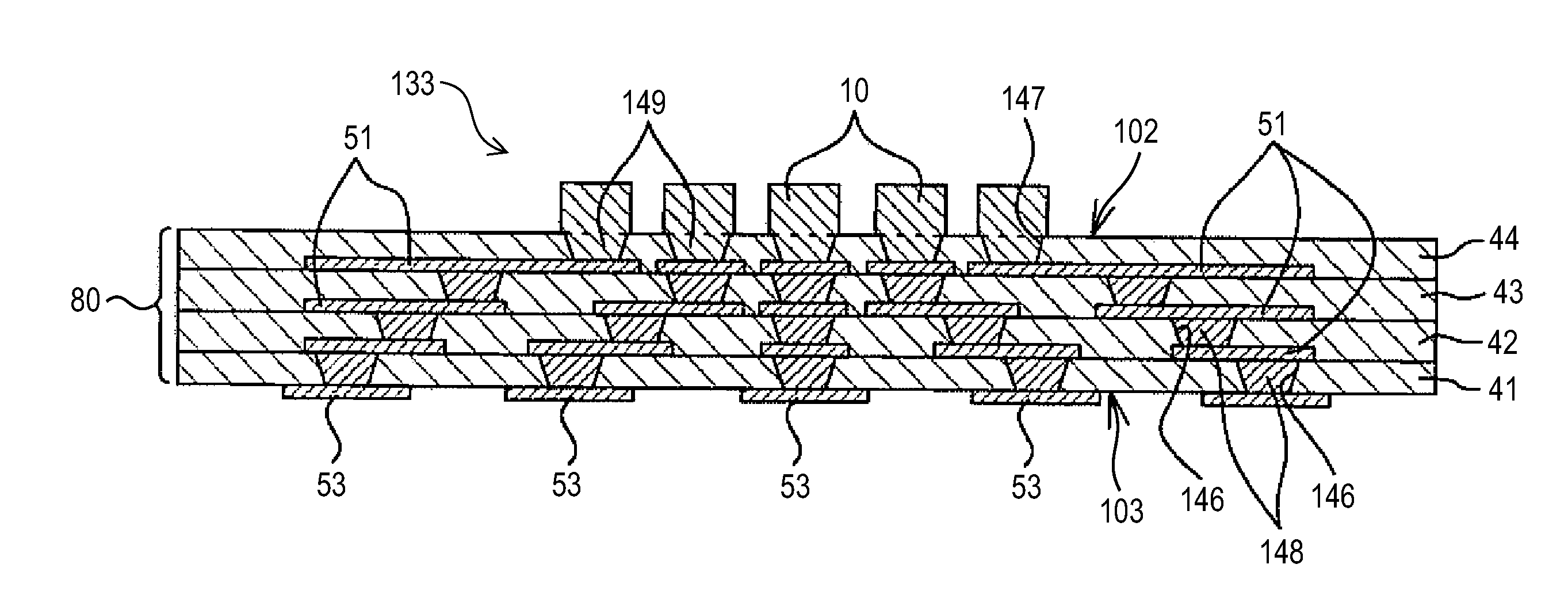
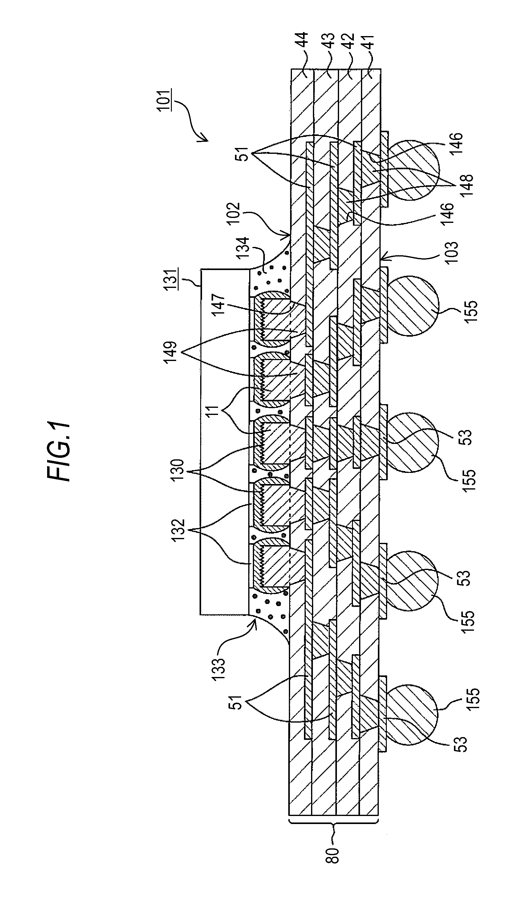
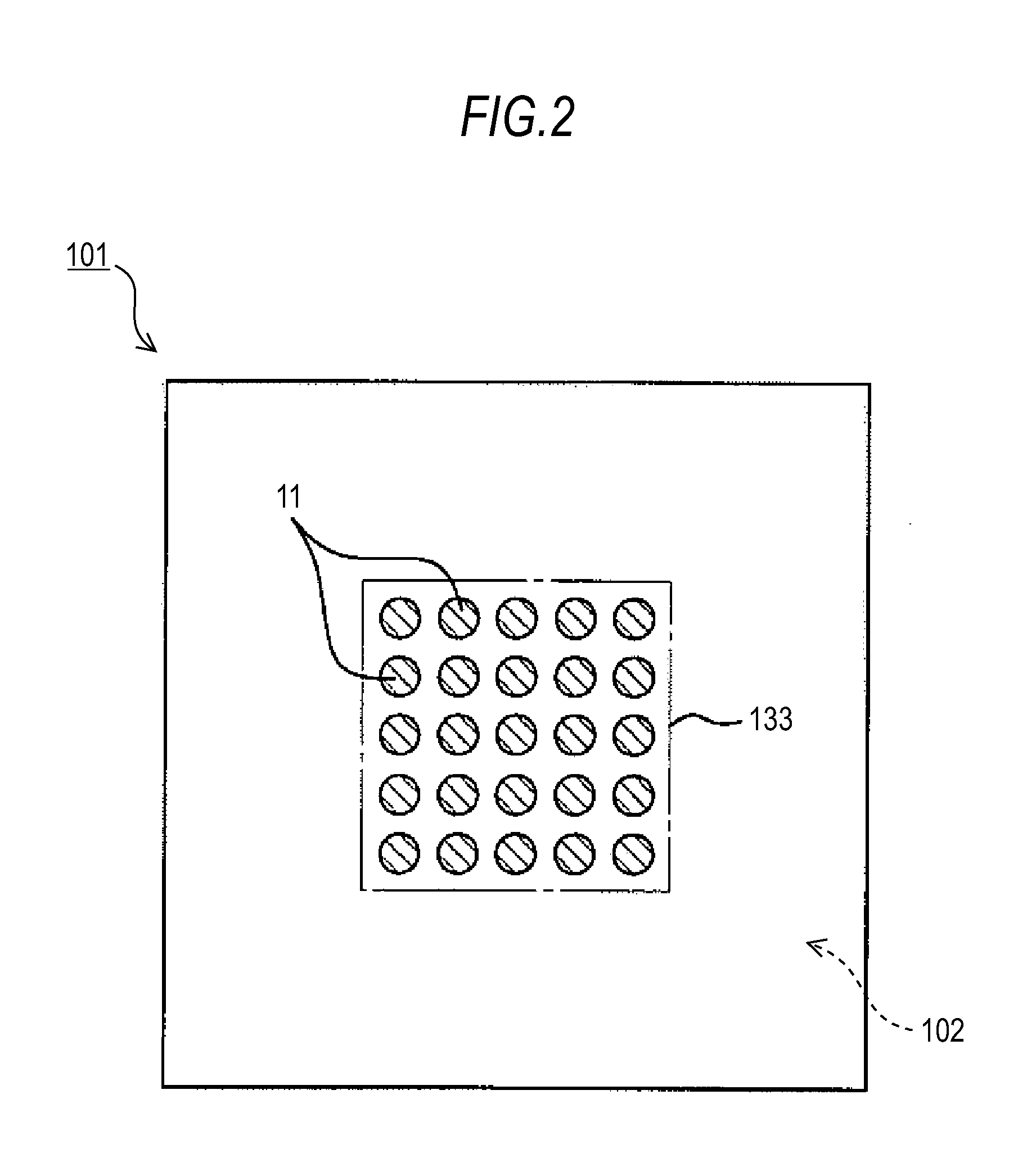
[0048]FIG. 1 is a schematic cross-sectional view illustrating a coreless wiring substrate 101 (wiring substrate) of the present embodiment. The coreless wiring substrate 101 does not have a core substrate and is a wiring substrate which has a structure where four layers of resin insulation layers 41, 42, 43 and 44 formed from an epoxy resin and conductor layers 51 formed from copper are alternately layered. The resin insulation layers 41 to 44 are interlayer insulation layers which have the same thickness and are formed from the same material.

[0049]Furthermore, each of the resin insulation layers 41 to 44 respectively includes via holes 146 and 147, and via conductors 148 and 149. Each of the via holes 146 and 147 has a reverse truncated cone shape and is formed by drilling with respect to each of the resin insulation layers 41 to 44 using a YAG laser or a c...


PUM

PropertyMeasurementUnit
Surface roughnessaaaaaaaaaa
Diameteraaaaaaaaaa

Abstract

Embodiments of the present invention provide a wiring substrate that includes a structure where a plurality of projection electrodes are arranged within an electrode formation region on a substrate main surface. At least one among the plurality of projection electrodes has a larger outer diameter than an outer diameter of a via conductor and is a variant projection electrode which has a roughened upper surface. Embodiments of the present invention also provide methods for manufacturing wiring substrates having one or more of said variant projection electrode.

Description

CROSS REFERENCE TO RELATED APPLICATION[0001]The present application claims priority from Japanese patent application 2011-233721, which was filed on Oct. 25, 2011, the disclosure of which is herein incorporated by reference in its entirety.BACKGROUND OF THE INVENTION[0002]1. Field of the Invention[0003]The present invention relates to a wiring substrate where a plurality of projection electrodes are arranged within an electrode formation region on a substrate main surface, and to a manufacturing method for the same.[0004]2. Description of Related Art[0005]In the related art, a wiring substrate (i.e., semiconductor package) formed by installing a component such as an IC chip is well known. Here, as a structure for enabling electrical connection to the IC chip, it has been proposed that a solder bump be formed on a plurality of connecting terminals arranged at the bottom surface side of the IC chip or on a pad (i.e., C4 pad: Controlled Collapsed Chip Connection Pad) which is a plurali...

Claims


Application Information

Patent Timeline
IPC IPC(8): H05K1/11H05K3/10
CPCH01L24/81H01L2224/16238H01L2224/81385H01L2224/81444H01L2224/81815H01L24/13H01L24/16H01L2224/32225H01L2224/73204H01L2924/15311H01L2924/01322H05K1/113H05K3/3436H05K3/4007H05K2203/0307H01L23/49811H01L23/49816H01L23/49822H01L23/49827H01L21/4853H01L21/486H05K3/4682H01L2224/13111H01L2224/81193H01L2924/1461Y10T29/49155H01L2224/16225H01L2924/00H01L2924/00014H01L2924/00012H01L2924/01082H01L2924/01047H01L2924/01083H01L2924/01029H01L2924/0103H01L2224/81192H01L2924/12042H01L23/12H05K3/46
Inventor INOUE, MASAHIROSUGIMOTO, ATSUHIKO
Owner NGK SPARK PLUG CO LTD
Why Eureka
Try Eureka