Epitaxial wafer and semiconductor device

a technology of semiconductor devices and epitaxial layers, applied in the direction of semiconductor devices, basic electric elements, electrical apparatus, etc., can solve the problems of deteriorating the crystal quality reducing increasing element resistance, etc., to prevent the decrease in the mobility of carriers, suppress the occurrence of crystal defects, and suppress the deterioration of the epitaxial layer due to crystal defects

Active Publication Date: 2013-04-25
MITSUBISHI ELECTRIC CORP
View PDF2 Cites 21 Cited by
  • Summary
  • Abstract
  • Description
  • Claims
  • Application Information

AI Technical Summary

Benefits of technology

[0018]An influence of a lattice constant difference between the semiconductor substrate and the epitaxial layer is mitigated, and occurrence of a crystal defect is suppressed. Even when a crystal defect occurs, deterioration in the crystal quality of the epitaxial layer due to the crystal defect is suppressed. This prevents decrease in the mobility of carriers in the drift layer 2. Thus, a semiconductor device having a low element resistance is achieved.

Problems solved by technology

This difference in the lattice constant (lattice mismatch) is a factor that causes a crystal defect, and thus deteriorates the crystal quality of the epitaxial layer particularly when the epitaxial layer has a large thickness.
Deterioration in the crystal quality of the epitaxial layer causes a problem that the mobility of carriers decreases and an element resistance increases.

Method used


Image

  • Epitaxial wafer and semiconductor device
  • Epitaxial wafer and semiconductor device
  • Epitaxial wafer and semiconductor device

Examples


embodiment 1

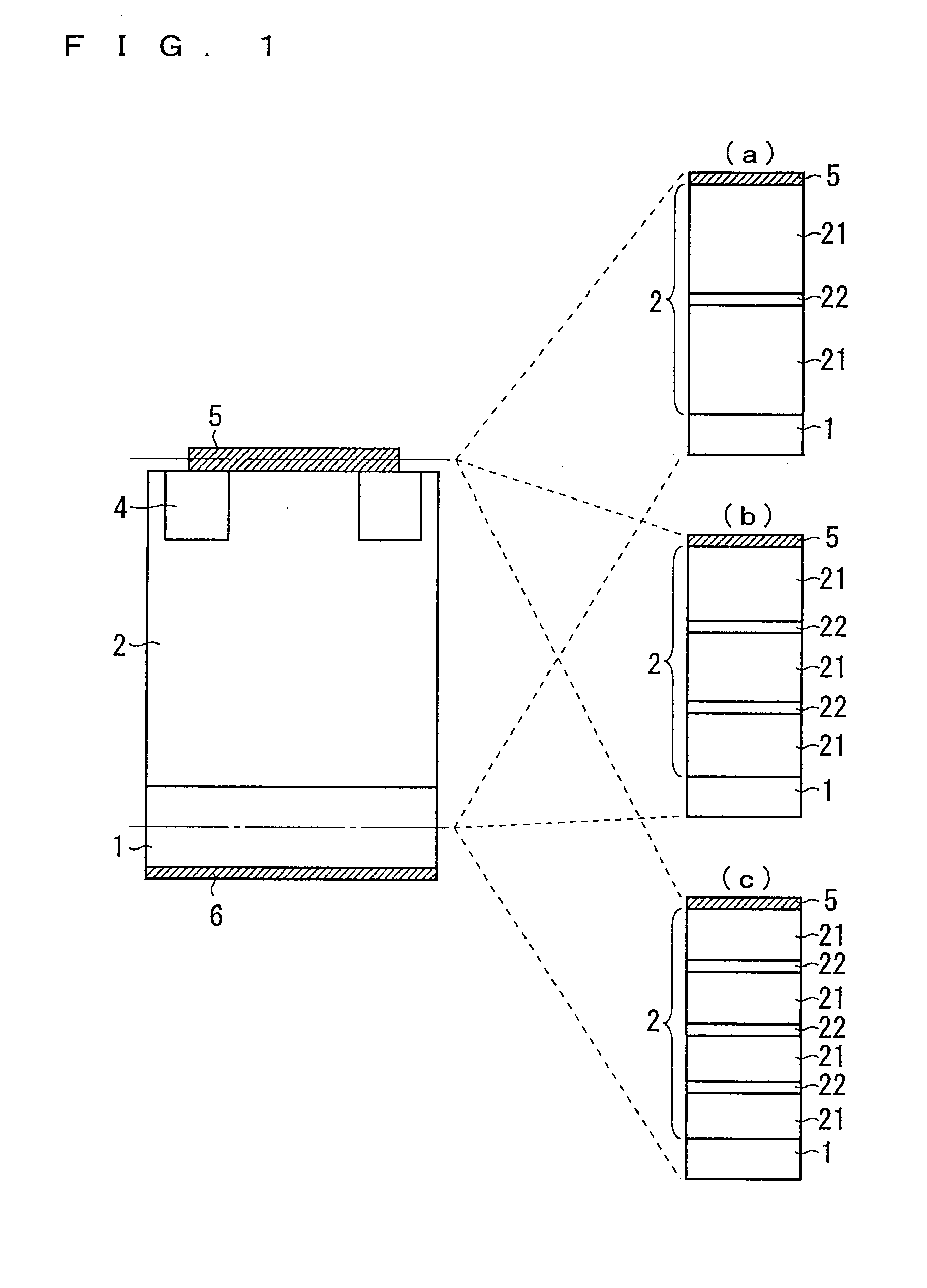
[0031]FIG. 1 is a diagram showing a configuration of a semiconductor device according to an embodiment 1 of the present invention, and illustrates a Schottky diode as an example. The parts (a) to (c) shown at the right in FIG. 1 indicate configurations of a drift layer (epitaxial layer) of the semiconductor device.

[0032]As shown in FIG. 1, the Schottky diode of this embodiment includes a substrate 1, a drift layer 2, a guard ring 4, an anode electrode 5, and a cathode electrode 6. The substrate 1 is a low resistance SiC substrate doped with an n-type dopant at a high concentration. In order to suppress the element resistance, it is desirable that the resistivity of the substrate 1 is as low as possible. Thus, a group-V element (such as nitrogen) is doped at a high concentration. However, when the doping concentration is excessively high, a crystal defect is likely to occur. Accordingly, the doping concentration is ordinarily set to be 1019 / cm3 and therearound, for example, to be abo...

embodiment 2

[0073]In an embodiment 2, a case where the present invention is applied to a field effect transistor is illustrated. FIG. 8 is a diagram showing a configuration of a field effect transistor that is a semiconductor element according to the embodiment 2. This field effect transistor is, similarly to the embodiment 1, formed with use of the epitaxial wafer 100 that includes the n-type SiC low resistance substrate 1 and the n-type SiC epitaxial layer 2a having the low concentration layer 21 and the ultrathin high concentration layer 22. The epitaxial layer 2a functions as the drift layer 2 of the field effect transistor.

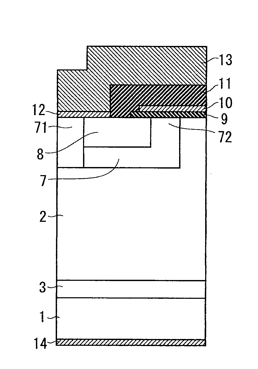
[0074]As shown in FIG. 8, the field effect transistor includes the substrate 1, the drift layer 2, a body region 7, a source region 8, a gate insulating film 9, a gate electrode 10, an interlayer insulating film 11, a source electrode 12, a interconnection 13, and a drain electrode 14. The drift layer 2 (epitaxial layer) provided on the substrate 1, similarly to the one ...

embodiment 3

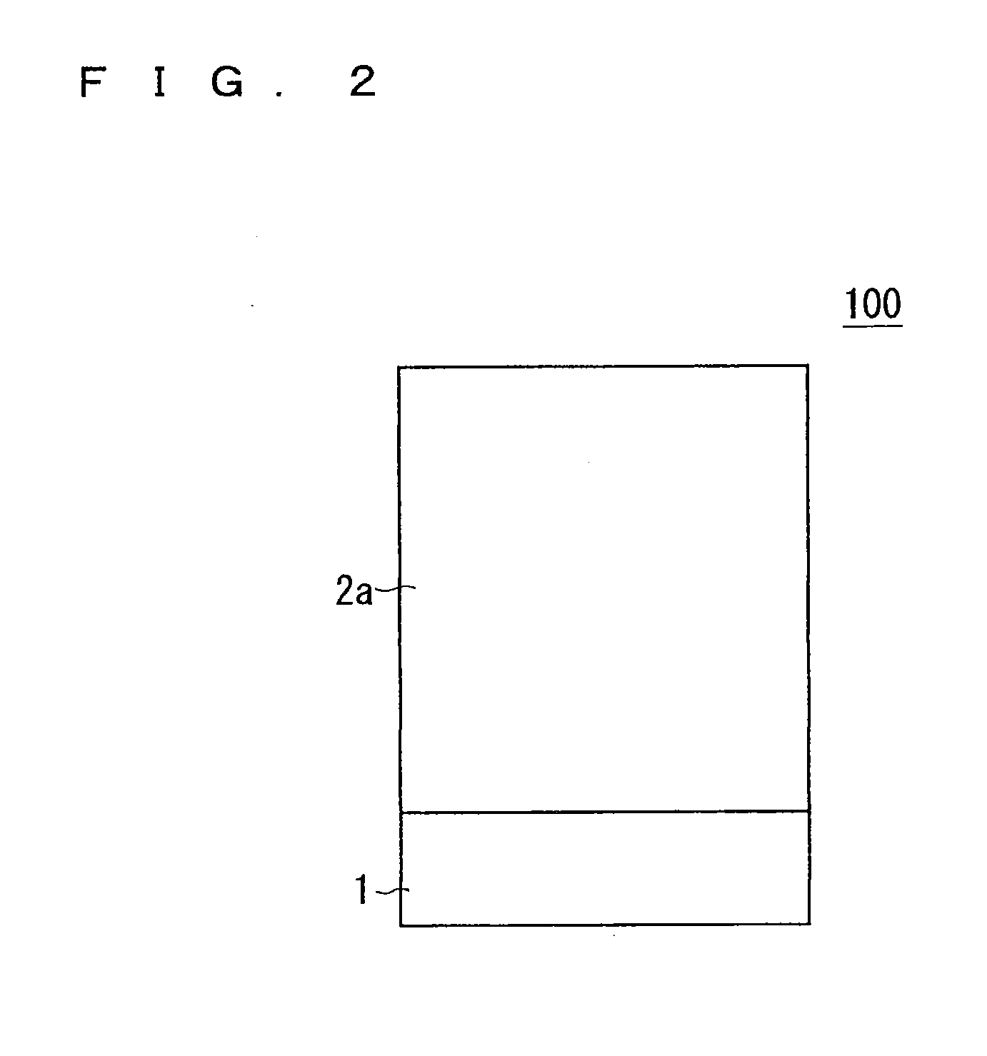
[0085]In the examples shown in the embodiments 1 and 2, the epitaxial wafer 100 is used in which the epitaxial layer 2a (the laminated structure of the low concentration layer 21 and the ultrathin high concentration layer 22) is grown immediately on the substrate 1 as shown in FIG. 2. Instead, in this embodiment, as shown in FIG. 10, an epitaxial wafer 101 having a buffer layer 3 provided between the substrate 1 and the epitaxial layer 2a is used.

[0086]Configurations of the substrate 1 and the epitaxial layer 2a are the same as those of the embodiments 1 and 2. The buffer layer 3 is a SiC layer whose doping concentration is set to be a value intermediate between the value of the substrate 1 and the value of the drift layer 2. Since the buffer layer 3 is interposed between the substrate 1 and the drift layer 2, occurrence of a crystal defect due to the lattice constant difference between the substrate 1 and the drift layer 2 can be further reduced.

[0087]The buffer layer 3 may have an...


PUM


Abstract

A semiconductor device that can suppress deterioration in crystal quality caused by a lattice mismatch between a substrate and an epitaxial layer and that also can ensure a voltage sustaining performance, and a wafer for forming the semiconductor device. An epitaxial wafer of silicon carbide (SiC), which is used for manufacturing a semiconductor device, includes a low resistance substrate and an epitaxial layer provided thereon. The epitaxial layer is doped with the same dopant as a dopant doped into the substrate, and has a laminated structure including a low concentration layer and an ultrathin high concentration layer. A doping concentration in the low concentration layer is lower than that in the silicon carbide substrate. A doping concentration in the ultrathin high concentration layer is equal to that in the silicon carbide substrate.

Description

TECHNICAL FIELD[0001]The present invention relates to an epitaxial wafer including a semiconductor substrate and an epitaxial layer grown thereon, and to a configuration of a semiconductor device formed with the same.BACKGROUND ART[0002]A semiconductor element including a silicon carbide (SiC) semiconductor is attracting attention as a device that can achieve a high breakdown voltage and a low loss. As a structure thereof, a structure in which an epitaxial layer formed on a substrate having a low resistance (high doping concentration) acts as an operating layer is widely known. Particularly, in a semiconductor element (power device) for power, an epitaxial layer functions as a voltage sustaining layer (drift layer). Conventionally, a single layer structure has been generally used for the epitaxial layer (for example, Patent Document 1).[0003]The epitaxial layer serving as a voltage sustaining layer of a power device ordinarily has a thickness of about 3 μm to 100 μm. However, depend...

Claims


Application Information

Patent Timeline
Patent Type & Authority Applications(United States)
IPC IPC(8): H01L29/16
CPCH01L21/02447H01L21/02529H01L21/0262H01L21/02573H01L29/66068H01L29/1608H01L21/02507H01L29/6606
Inventor OHTSUKA, KENICHITOMITA, NOBUYUKIFURUSHO, TOMOAKI
Owner MITSUBISHI ELECTRIC CORP
Why Eureka
Try Eureka