
Via structures and compact three-dimensional filters with the extended low noise out-of-band area

a three-dimensional filter and compact technology, applied in the field ofvia structures and filters, can solve problems such as suppression of unwanted resonant modes, and achieve the effect of improving suppression of undesirable resonant modes

Active Publication Date: 2013-04-25
NEC CORP
View PDF2 Cites 13 Cited by
  • Summary
  • Abstract
  • Description
  • Claims
  • Application Information

AI Technical Summary

Benefits of technology

The present invention aims to provide smaller filters in multilayer substrates that can better suppress the unwanted resonant mode in the out-of-band area. Additionally, the invention improves the filter's skirt or sharpness while maintaining its size.

Problems solved by technology

However, there are crucial problems in filter design, namely suppressions of unwanted resonant modes in the out-of-band area.

Method used


Image

  • Via structures and compact three-dimensional filters with the extended low noise out-of-band area
  • Via structures and compact three-dimensional filters with the extended low noise out-of-band area
  • Via structures and compact three-dimensional filters with the extended low noise out-of-band area

Examples


Embodiment Construction

[0059]Hereinafter, several embodiments of via structures and filters disposed in multilayer substrates according to the present invention will be described in details with reference to attached drawings. But, it would be well understood that this description should not be viewed as narrowing the appended claims.

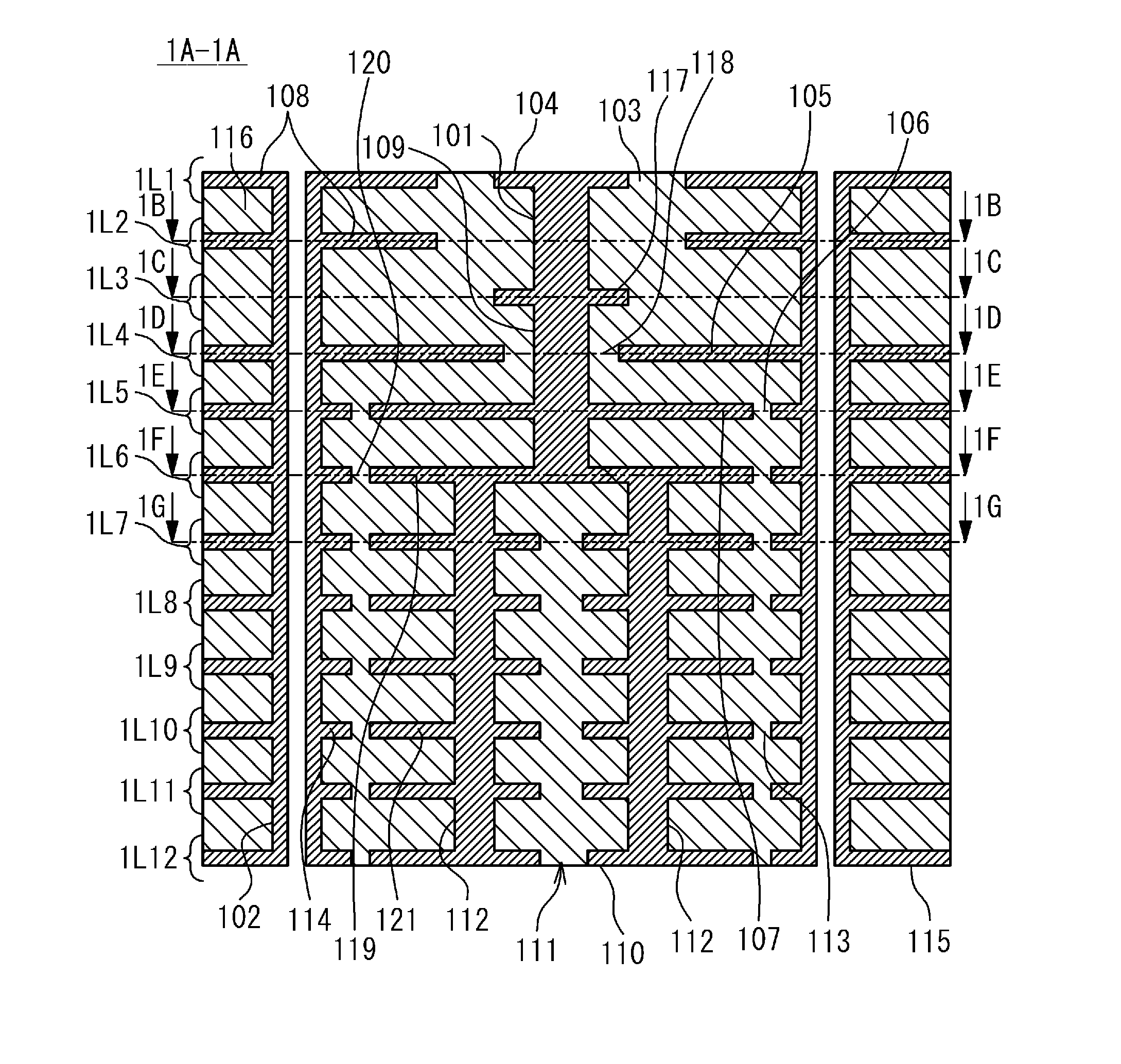
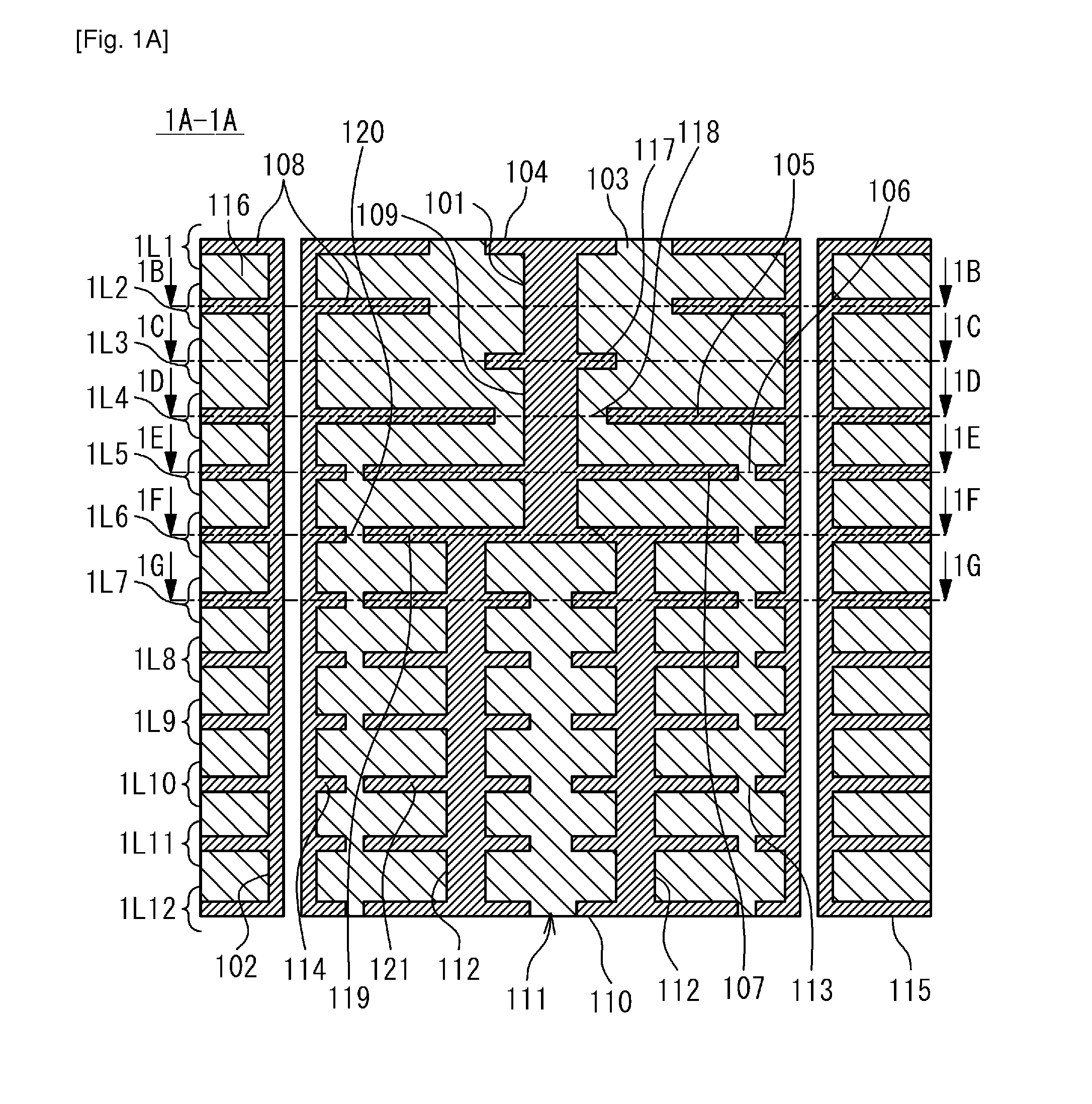
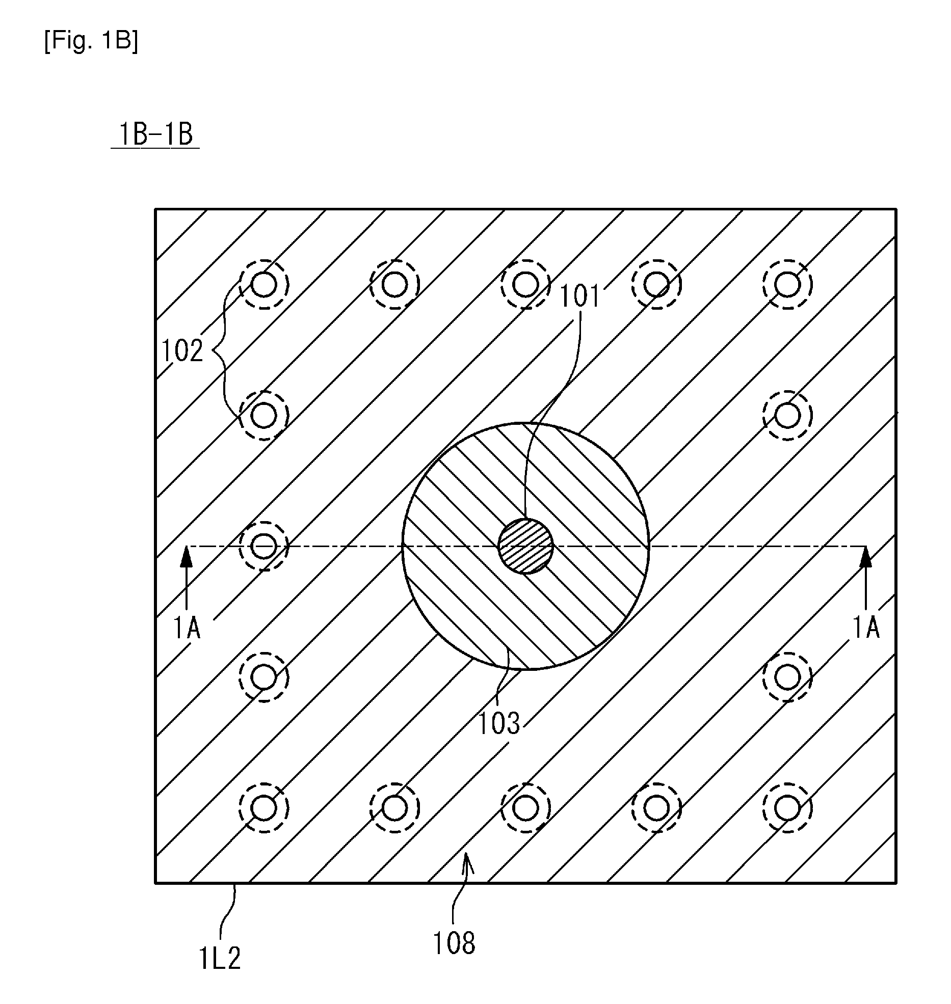
[0060]In FIGS. 1A to 1I, an exemplary embodiment of a via structure in a twelve-conductor-layer substrate of the present invention is shown.

[0061]It should be noted that this twelve-conductor-layer substrate is only an example of multilayer substrates and a number of conductor layers, filling material and other substrate parameters can be different that depends on applications.

[0062]The multilayer substrate shown in FIGS. 1A to 1I is provided with twelve stacked conductor layers 1L1, 1L2, 1L3, 1L4, 1L5, 1L6, 1L7, 1L8, 1L9, 1L10, 1L11 and 1L12, and those twelve conductor layers are isolated by a dielectric 116.

[0063]In present embodiment, the via structure has three functional...


PUM


Abstract

A filter of the present invention includes a plurality of via structures with a multilayer substrate. Each of the plurality of via structures includes first, second and third functional sections. One end of a signal via of the first functional section is connected to one end of a signal via of the second functional section and another end of the signal via of the second functional section is connected to two signal vias of the third functional section. Those signal vias are surrounded by a plurality of ground vias. Input and output ports of the filter are connected to another end of the signal via of each first functional section.

Description

TECHNICAL FIELD [0001]The present invention relates to via structures and filters based on multilayer substrate technologies.BACKGROUND ART [0002]Filtering components are one of key elements in modern and next-generation networking and computing equipment because they are responsible for controlling the frequency responses. For practical applications, it is important to obtain such structures as compact, cost-effective and low energy consuming devices. Also, filters have to be easily integrated in a system.[0003]Multilayer substrates are low-cost interconnect technologies. That is why they are used as the basis of chip, package and printed circuit board constructions forming networking and computing systems.[0004]Transmission lines in multilayer substrates can be implemented as horizontal and vertical wave guiding structures.[0005]Microstrip lines, striplines, parallel plate lines and coplanar waveguides are some typical representatives of planar (horizontal) transmission lines.[000...

Claims


Application Information

Patent Timeline
Patent Type & Authority Applications(United States)
IPC IPC(8): H01P1/213
CPCH01P1/203H05K1/0222H05K1/0233H05K1/0251H01P1/20H05K3/4614H05K2201/09609H05K2201/09618H05K2201/0979H05K3/429
Inventor KUSHTA, TARAS
Owner NEC CORP
Learn More